This engineering guide explains the complete flyback transformer design process, including operating modes, energy storage, magnetizing inductance, peak current, turns ratio, core and material selection, air-gap design, winding construction, leakage inductance, losses, thermal performance, a worked example, and automated design tools.
In This Guide — Click to Expand
1. What Is a Flyback Transformer?
A flyback transformer is the magnetic energy-storage element used in a flyback converter. Although it is commonly called a transformer, its magnetic behavior differs in an important way from that of a conventional power transformer.
In a conventional transformer, energy is transferred from the primary winding to the secondary winding while both windings are magnetically coupled through the core. Ideally, very little energy is intentionally stored in the magnetic field.
A flyback transformer operates differently. During the switch ON interval, current increases in the primary winding and energy is stored in the transformer’s magnetizing inductance. During this interval, the secondary rectifier is normally reverse biased and energy is not delivered through the secondary winding in the idealized flyback model.
When the primary switch turns OFF, the winding voltages reverse polarity, the secondary rectifier becomes forward biased, and the stored magnetic energy is transferred through the secondary winding to the output.
Because the magnetic component must intentionally store energy, a flyback transformer behaves in many respects like a coupled energy-storage inductor rather than a conventional transformer.
This distinction has major consequences for the magnetic design.
A practical flyback transformer must simultaneously provide:
- The required magnetizing inductance
- Sufficient energy-storage capability
- Primary-to-secondary voltage transformation
- Galvanic isolation when required
- Adequate saturation margin
- Acceptable core and winding losses
- Appropriate creepage and clearance
- Practical winding geometry and window utilization
- Acceptable leakage inductance and parasitic capacitance
- Thermal performance across the operating range
- Manufacturable mechanical construction
Unlike a conventional transformer, a flyback transformer commonly uses an intentional air gap in the magnetic path. The gap reduces the effective permeability of the magnetic circuit, allows the required magnetizing inductance to be established with an appropriate number of turns, and increases the magnetic circuit’s usable energy-storage capability.
Conventional Transformer vs. Flyback Transformer
| Conventional Transformer | Flyback Transformer |
|---|---|
| Primarily transfers energy between windings | Stores energy and subsequently transfers it |
| Primary and secondary power transfer occurs simultaneously in the ideal model | Primary energy-storage and secondary energy-delivery intervals occur at different times |
| Usually designed for relatively little intentional magnetic energy storage | Magnetizing inductance intentionally stores substantial energy |
| Often ungapped or only minimally gapped | Commonly uses an intentional air gap |
| Magnetizing current is generally undesirable and minimized | Magnetizing current is fundamental to operation |
| Design emphasizes turns ratio, flux, losses, and isolation | Design must also coordinate energy storage, peak current, magnetizing inductance, and gap |

SolidMag Engineering Insight
A flyback transformer should not be approached as a conventional transformer with an air gap added afterward. Magnetizing inductance, stored energy, peak current, core geometry, turns, air gap, winding arrangement, isolation, leakage inductance, losses, and temperature are interconnected design variables.
Changing one of these parameters can affect several others. Successful flyback transformer design therefore requires the magnetic component to be treated as a complete electrical, magnetic, thermal, mechanical, and manufacturing system.
2. How Does a Flyback Converter Transfer Energy?
Understanding the switching sequence is fundamental to flyback transformer design because the primary and secondary windings perform different functions during different portions of each switching cycle.
A simplified flyback switching cycle can be divided into two primary intervals.
Switch ON — Energy Storage
When the primary MOSFET turns ON, the input voltage is applied across the primary winding.
Primary current begins increasing according to the magnetizing inductance of the transformer. As this current rises, magnetic energy is stored in the coupled magnetic structure.
During the idealized ON interval:
- Input voltage is applied to the primary winding.
- Primary magnetizing current increases.
- Magnetic flux increases in the core.
- Energy stored in the magnetizing inductance increases.
- The secondary winding polarity keeps the output rectifier reverse biased.
- The output capacitor supplies the load while the transformer is storing energy.
The slope of the primary magnetizing current is determined primarily by the applied primary voltage and magnetizing inductance.
Switch OFF — Energy Delivery
When the MOSFET turns OFF, current in the magnetizing inductance cannot change instantaneously.
The winding voltages therefore reverse polarity. The secondary rectifier becomes forward biased, and the magnetic energy stored during the ON interval begins flowing through the secondary winding into the output circuit.
During the idealized OFF interval:
- The primary switch is OFF.
- Primary switch current falls to zero apart from parasitic/transient effects.
- Winding voltages reverse polarity.
- The secondary rectifier conducts.
- Secondary current delivers stored magnetic energy to the output.
- Magnetizing current referred to the secondary decreases as the stored energy is removed.
- Core flux decreases toward its next-cycle value.
The process then repeats during the next switching cycle.

Why This Matters to Transformer Design
The transformer must be designed for both portions of the switching cycle.
The primary winding must withstand the required peak and RMS current while producing an acceptable flux excursion in the core.
The secondary winding must carry the corresponding energy-delivery current while maintaining acceptable copper loss, current density, temperature rise, insulation, and mechanical fit.
At the same time, the turns ratio must establish an appropriate reflected voltage, the air gap and turns must establish the required magnetizing inductance, and the core must remain within acceptable flux-density and loss limits.
The flyback transformer therefore cannot be designed from turns ratio alone. Its electrical and magnetic requirements are determined by the complete switching cycle.
SolidMag Engineering Insight
The two switching intervals should always be considered together. Increasing the energy stored during the ON interval changes the peak primary current, flux excursion, magnetizing inductance requirement, secondary current, winding loss, and energy that must be delivered during the OFF interval.
Flyback transformer design is therefore fundamentally an energy-per-switching-cycle problem, not simply a voltage-ratio problem.
3. CCM, DCM, and Boundary Mode in Flyback Converters

A flyback converter may operate in discontinuous conduction mode (DCM), boundary conduction mode (BCM), or continuous conduction mode (CCM).
The distinction is based on the behavior of the magnetizing current from one switching cycle to the next.
This operating mode directly affects magnetizing inductance, peak and RMS current, transformer energy storage, semiconductor stresses, control behavior, and magnetic-component design.
Discontinuous Conduction Mode — DCM
In DCM, the energy stored in the magnetizing inductance is completely transferred to the secondary before the next switching cycle begins.
The magnetizing current therefore returns to zero and remains at zero for a finite interval before the primary switch turns ON again.
DCM generally produces:
- Higher peak current for a given power level
- Higher RMS winding current
- Complete demagnetization of the transformer each cycle
- A clearly defined zero-current interval
- Potentially simpler energy-per-cycle analysis
- Increased semiconductor and winding current stress compared with an equivalent lower-peak-current design
DCM is common in lower-power flyback converters and in converters that intentionally operate discontinuously over some or all of the load range.
Boundary Conduction Mode — BCM
Boundary conduction mode, also called critical conduction mode (CrCM), occurs at the boundary between DCM and CCM.
In BCM, the magnetizing current falls to zero at approximately the instant the next switching cycle begins.
There is therefore no significant zero-current dead time, but there is also no residual magnetizing current carried into the next cycle.
BCM can provide useful switching characteristics in some converter implementations but often requires variable-frequency or specialized control strategies.
Continuous Conduction Mode — CCM
In CCM, the magnetizing current does not return to zero before the next primary switching interval begins.
Some magnetizing current therefore remains from the previous switching cycle.
Compared with DCM, CCM can reduce peak current for a given power level, which can reduce conduction stress in the windings and semiconductor devices.
However, CCM changes the converter dynamics and control requirements and may increase stored magnetic energy at a given operating point.
The transformer must be designed for the resulting DC bias, current ripple, flux excursion, RMS current, and worst-case peak current.
Comparing Flyback Operating Modes
| Characteristic | DCM | BCM | CCM |
|---|---|---|---|
| Magnetizing current reaches zero | Yes, for a finite interval | Yes, at the cycle boundary | No |
| Residual current at next cycle | None | Approximately zero | Present |
| Peak current for comparable power | Generally higher | Intermediate | Generally lower |
| Zero-current interval | Present | Essentially zero | None |
| Transformer completely demagnetizes each cycle | Yes | Approximately yes | No |
| Control behavior | Relatively straightforward in many low-power designs | Often variable-frequency / boundary-controlled | More complex dynamics |
| Common use | Many low-power flyback converters | Boundary/critical-mode converters | Higher-power or lower-peak-current flyback designs |
These are general tendencies rather than universal rules. Actual performance depends on input voltage, output power, switching frequency, magnetizing inductance, duty cycle, turns ratio, semiconductor selection, and control method.
SolidMag Engineering Insight
Operating mode should be established early in the flyback design process because it directly influences the magnetizing-inductance target and current waveform used to size the transformer.
A transformer optimized for DCM should not automatically be assumed suitable for CCM operation, and vice versa. Peak current, RMS current, stored energy, magnetic bias, flux excursion, winding loss, semiconductor stress, and control behavior must be evaluated for the actual operating mode across the complete input-voltage and load range.
4. What Inputs Are Required to Design a Flyback Transformer?

A practical flyback transformer cannot be designed from output voltage, output power, and turns ratio alone.
The magnetic component must operate across the converter’s complete electrical and environmental operating envelope. The designer therefore needs enough information to determine stored energy, magnetizing inductance, peak and RMS currents, turns ratio, flux density, core size, winding construction, insulation requirements, losses, temperature rise, and mechanical fit.
The most important design inputs typically include:
| Design Input | Why It Matters |
|---|---|
| Minimum input voltage | Often drives maximum duty cycle and high primary current |
| Maximum input voltage | Affects duty cycle, primary volt-seconds, switching stress, and flux conditions |
| Output voltage | Helps determine turns ratio and secondary winding requirements |
| Output current / power | Determines required energy transfer and winding-current requirements |
| Switching frequency | Determines energy per cycle and strongly influences core and winding losses |
| Target efficiency | Determines required input power and influences thermal design |
| Maximum duty cycle | Constrains turns ratio, reflected voltage, flux excursion, and control margin |
| Operating mode | Determines magnetizing-current behavior and strongly affects the inductance target |
| Allowed current ripple | Influences magnetizing inductance and peak-current requirements |
| Ambient temperature | Establishes available thermal margin |
| Maximum temperature rise | Limits allowable core and winding losses |
| Isolation voltage | Influences insulation system, creepage, clearance, bobbin, and winding construction |
| Winding preferences | Affects conductor selection, fill, AC resistance, leakage, and manufacturability |
| Mechanical envelope | Limits allowable core, bobbin, winding, and package dimensions |
| Core/material preferences | Constrains candidate magnetic solutions |
| EMI priorities | Can influence winding arrangement, interleaving, shielding, and parasitic capacitance |
| Cost / size / efficiency priorities | Determines how candidate designs should be optimized |
Why Worst-Case Conditions Matter
Flyback transformer design should not be based only on nominal operating conditions.
Different constraints may become critical at different corners of the operating envelope.
For example:
- Minimum input voltage may produce the highest primary current.
- Maximum input voltage may produce important voltage-stress or flux considerations depending on the control strategy.
- Maximum output power generally increases winding and thermal stress.
- High ambient temperature reduces available thermal margin.
- Component tolerances can change magnetizing inductance and peak current.
- Switching-frequency tolerance can alter flux excursion, loss, and energy-per-cycle requirements.
A robust design therefore evaluates multiple operating corners rather than optimizing the transformer around a single nominal point.
Design Priorities Are Inputs Too
Two transformers satisfying the same electrical requirements may look very different if one design prioritizes efficiency while another prioritizes minimum size or minimum cost.
Practical optimization may include priorities such as:
- Efficiency
- Physical size
- Temperature rise
- Cost
- EMI
- Power density
- Reliability
- Manufacturability
These priorities should influence candidate selection rather than being treated as cosmetic preferences after the transformer has already been designed.
SolidMag Engineering Insight
A flyback transformer is the result of an interacting set of electrical, magnetic, thermal, mechanical, insulation, and manufacturing constraints.
The quality of the final design therefore depends heavily on the quality of the requirements supplied at the beginning of the process.
This is why SolidMagnetics begins automated flyback transformer design with the converter requirements and design priorities rather than asking the user to choose a core and winding configuration first.
Have Your Flyback Requirements Ready?
Enter your electrical, magnetic, thermal, mechanical, and design-priority requirements into the SolidMagnetics Flyback Transformer Designer and evaluate an automated design.
5. How Much Energy Must the Transformer Store?
Energy storage is one of the defining requirements of a flyback transformer. During the primary switch ON interval, energy is accumulated in the transformer’s magnetizing inductance. When the switch turns OFF, that stored energy is transferred through the secondary winding to the output.
For a magnetizing inductance Lm carrying current I, the stored magnetic energy is:
Where:
- E = stored magnetic energy, J
- Lm = primary-referred magnetizing inductance, H
- I = instantaneous primary magnetizing current, A
At the maximum primary current:
This relationship illustrates one of the most important flyback design trade-offs: stored energy increases linearly with magnetizing inductance but with the square of peak current.
A relatively small increase in peak current can therefore produce a substantial increase in the energy that the magnetic structure must accommodate.
Energy Per Switching Cycle
In an idealized DCM flyback converter that completely demagnetizes each cycle, the energy stored during each switching cycle is transferred to the secondary before the next cycle begins.
A useful first-pass input-power relationship is therefore:
Where:
- PIN = input power, W
- fs = switching frequency, Hz
If converter efficiency is represented by η:
This form is particularly useful for understanding DCM energy transfer, but it should not be applied blindly to CCM operation. In CCM, magnetizing current does not return to zero each cycle, so power transfer depends on the incremental change in stored magnetic energy between the beginning and end of the switching interval.
For a current that changes from IMIN to IMAX, the incremental stored-energy change is:
This distinction is one reason the operating mode established in Section 3 matters so much to the transformer design.
Energy Storage and the Magnetic Core
The required energy cannot be considered independently of the physical magnetic structure.
Core cross-sectional area, magnetic path length, air gap, turns, saturation limit, material characteristics, and allowable flux density all affect how the required magnetizing inductance and energy storage can be realized.
In a deliberately gapped ferrite flyback transformer, much of the incremental magnetic-field energy associated with energy storage is concentrated in the air-gap region. The core, turns, and gap must therefore be designed together rather than selecting a core first and adding whatever gap happens to produce the desired inductance.
SolidMag Engineering Insight
Energy per switching cycle is one of the fundamental sizing quantities in flyback transformer design.
Output power alone does not determine transformer size. Switching frequency, operating mode, magnetizing inductance, peak current, allowable flux density, air gap, winding losses, and thermal limits determine how that power must be processed by the magnetic component.
Two flyback converters delivering the same output power can therefore require substantially different transformers.
6. How Is Magnetizing Inductance Selected?
Magnetizing inductance, Lm, is one of the central design parameters of a flyback transformer because it determines how rapidly primary current changes when voltage is applied to the winding.
During the primary switch ON interval, the idealized current slope is:
For approximately constant input voltage during an ON interval of duration tON:
Since:
the primary-current change can also be expressed as:
Where:
- VIN = voltage applied across the primary winding
- D = duty cycle
- fs = switching frequency
- Lm = primary-referred magnetizing inductance
- ΔIP = primary magnetizing-current change during the ON interval
What Happens if Magnetizing Inductance Is Too Low?
For the same input voltage, duty cycle, and switching frequency, reducing Lm increases the primary-current ramp.
This can lead to:
- Higher peak primary current
- Higher RMS primary current
- Increased MOSFET conduction stress
- Increased copper loss
- Greater current-sense requirements
- Potential saturation problems if turns and gap are not adjusted appropriately
However, lower magnetizing inductance can also be consistent with intentional DCM operation and may allow the required energy to be transferred using a particular switching strategy.
What Happens if Magnetizing Inductance Is Too High?
Increasing Lm reduces the primary-current ripple for the same applied volt-seconds.
Depending on operating mode and power level, excessive magnetizing inductance can lead to:
- Greater residual current in CCM
- Different required turns/gap combinations
- Increased stored energy associated with bias current
- Changed transient and control behavior
- Increased sensitivity to some operating tolerances
- A magnetic design that becomes difficult to realize within the available core and winding window
Therefore, “higher inductance” is not automatically better.
Magnetizing Inductance Depends on Operating Mode
In DCM, current begins at approximately zero each cycle, making ΔIP approximately equal to IPK.
In CCM:
while:
The same current-ramp equation therefore applies, but the total current waveform is offset by the residual magnetizing current.
This distinction affects:
- Peak current
- RMS current
- Stored energy
- Core bias
- Copper loss
- Control behavior
- Saturation margin
Magnetizing-Inductance Tolerance Matters
The calculated nominal inductance is not the only value the converter will encounter.
Magnetizing inductance can vary because of:
- Core permeability tolerance
- Air-gap tolerance
- Number-of-turns tolerance
- Assembly variation
- Temperature
- Operating flux level
- Manufacturing variation
Worst-case Lm should therefore be evaluated when calculating peak current and saturation margin.
SolidMag Engineering Insight
Magnetizing inductance should be selected from the required current waveform and operating mode—not chosen independently as a transformer specification.
The correct Lm is the value that allows the converter to transfer the required energy while satisfying peak-current, RMS-current, saturation, loss, control, winding, and thermal constraints across the complete operating envelope.
7. How Is Peak Primary Current Calculated?
Peak primary current is one of the most important quantities in flyback transformer and converter design.
It directly influences:
- Required magnetic energy storage
- Core saturation margin
- Primary conductor size
- Primary winding copper loss
- MOSFET current rating
- Current-sense range
- Switching stress
- Air-gap and turns requirements
- Thermal performance
Peak current must therefore be evaluated at the operating condition that produces the highest current—not simply at nominal input voltage and nominal load.
The method used to calculate peak current depends strongly on whether the converter operates in discontinuous conduction mode (DCM), boundary conduction mode (BCM), or continuous conduction mode (CCM).
Peak Primary Current in DCM
In idealized discontinuous conduction mode, the primary magnetizing current begins each switching cycle at approximately zero.
The primary current rises during the MOSFET ON interval from zero to its peak value. Therefore:
Using the primary-current ramp relationship developed in Section 6:
where:
- IPK = peak primary magnetizing current
- VIN = voltage applied across the primary winding
- D = duty cycle
- Lm = primary-referred magnetizing inductance
- fs = switching frequency
This form is useful when duty cycle and magnetizing inductance are already known.
Calculating DCM Peak Current from Power
In an idealized DCM flyback converter that completely demagnetizes during every switching cycle, the energy stored at peak primary current is:
If this energy is transferred once per switching cycle, the approximate input power is:
Solving for peak current gives:
When estimated converter efficiency is included:
These relationships provide useful first-pass estimates for DCM operation. Real designs must also account for losses, tolerances, switching behavior, control strategy, and the actual operating waveform.
Peak Primary Current in BCM
Boundary conduction mode represents the transition between DCM and CCM.
Ideally, the magnetizing current falls to approximately zero just as the next switching cycle begins. Therefore, the primary current during the ON interval again rises from approximately zero to its peak value.
As a result:
However, unlike fixed-frequency DCM operation, many BCM controllers vary switching frequency as input voltage and load change.
Peak current should therefore be evaluated using the actual control strategy and switching frequency at each important operating condition.
Peak Primary Current in CCM
Continuous conduction mode requires a different treatment.
In CCM, the magnetizing current does not return to zero before the next switching cycle begins. The primary current therefore starts the MOSFET ON interval at a nonzero value IMIN and rises to IMAX.
The current ripple is:
The current change produced during the primary ON interval is still:
The peak primary current is therefore:
If the triangular current ripple is described relative to its average magnetizing current IAVG, then:
This distinction is important.
The DCM energy-per-cycle equation should not simply be reused to calculate CCM peak current because the transformer begins each CCM switching cycle with residual magnetizing current and stored magnetic energy.
The CCM current waveform must instead be determined from the converter operating point, magnetizing inductance, duty cycle, switching frequency, load, and control strategy.
Why Minimum Input Voltage Often Produces High Peak Current
For many regulated flyback converters, minimum input voltage requires greater input current to deliver the same output power.
The controller may also increase duty cycle as input voltage decreases.
These effects frequently make minimum input voltage at maximum load an important peak-current design condition.
However, low-line/full-load operation should not automatically be assumed to be the only worst-case condition.
The actual maximum peak current can also depend on:
- Converter operating mode
- Control strategy
- Maximum duty-cycle limit
- Switching-frequency variation
- Magnetizing-inductance tolerance
- Converter efficiency
- Current-limit implementation
- Load transients
- Input-voltage transients
- Startup conditions
A robust design evaluates peak current across the complete operating envelope.
Magnetizing-Inductance Tolerance Affects Peak Current
The nominal value of Lm is not necessarily the value that produces the highest current.
From the current-ramp relationship:
a reduction in magnetizing inductance produces a steeper current ramp when the other variables remain constant.
Therefore, the minimum expected magnetizing inductance is an important condition to evaluate when determining worst-case peak current.
Magnetizing-inductance variation can result from:
- Air-gap tolerance
- Core permeability variation
- Manufacturing tolerances
- Assembly variation
- Temperature
- Magnetic operating point
This is why the nominal calculated current should not be used as the sole basis for saturation or semiconductor-current margin.
Peak Current and Core Saturation
The transformer must support the worst-case primary current without driving the magnetic core into an unacceptable saturation region.
Peak current, however, cannot be evaluated independently from:
- Primary turns
- Core cross-sectional area
- Air gap
- Magnetizing inductance
- Core material
- Operating temperature
- Flux-density excursion
These relationships will be developed further in the following sections when we calculate primary turns, flux density, and air gap.
For now, the important point is that electrical peak current establishes one of the principal magnetic design constraints.
Allow Margin Above the Calculated Peak Current
A production design should not place the normal calculated peak current directly at the core saturation limit, semiconductor current limit, or current-sense limit.
Appropriate margin should be considered for:
- Magnetizing-inductance tolerance
- Input-voltage variation
- Output-load variation
- Load transients
- Current-sense tolerance
- Controller propagation delay
- Switching-frequency tolerance
- Air-gap tolerance
- Temperature effects
- Core-property variation
The appropriate margin depends on the converter architecture, controller, protection strategy, magnetic material, operating environment, and reliability requirements.
SolidMag Engineering Insight
Peak Current Is Where the Electrical and Magnetic Designs Meet
The converter determines the required primary-current waveform, but the transformer must physically accommodate that current without excessive flux density, winding loss, temperature rise, or saturation.
This makes peak primary current one of the most important links between the converter design and the magnetic design.
A flyback transformer that satisfies nominal output-power requirements but cannot safely accommodate the worst-case peak primary current is not a robust design.
Peak current should therefore be verified across input voltage, output load, switching frequency, magnetizing-inductance tolerance, temperature, and other relevant worst-case operating conditions before the magnetic design is finalized.
8. How Is the Flyback Turns Ratio Selected?
The turns ratio of a flyback transformer affects much more than the relationship between primary and secondary voltage.
It influences:
- Reflected voltage on the primary
- MOSFET voltage stress
- Secondary rectifier reverse-voltage stress
- Primary and secondary current levels
- Duty cycle
- Transformer demagnetization time
- Winding turns
- Copper loss
- Leakage inductance
- Winding capacitance
- Window utilization
For this reason, the turns ratio should be selected as part of the complete converter design rather than by applying the ordinary transformer voltage-ratio equation alone.
Reflected Output Voltage
When the primary switch turns OFF and the secondary rectifier conducts, the secondary output voltage is reflected back to the primary according to the winding turns ratio.
For a primary-to-secondary turns ratio:
an approximate primary-referred reflected voltage is:
Where:
- VR = secondary output voltage reflected to the primary
- NP = primary turns
- NS = secondary turns
- VO = regulated output voltage
- VD = secondary rectifier forward-voltage drop
The reflected voltage becomes an important part of the primary-switch voltage stress during the OFF interval.
Ignoring leakage-inductance overshoot, ringing, clamp action, and other transient effects:
A practical MOSFET selection must also provide margin for:
- Maximum input voltage
- Leakage-inductance voltage spike
- Clamp or snubber operating voltage
- Parasitic ringing
- Component tolerances
- Startup and transient behavior
- Required semiconductor derating
General Flyback Volt-Second Balance
In steady-state operation, the positive primary volt-seconds applied during the MOSFET ON interval must be balanced by the negative reflected volt-seconds applied while the secondary winding conducts.
The general idealized relationship is:
Define:
and:
where:
- D = primary switch ON-time fraction
- DS = secondary conduction fraction
- Ts = switching period
- VP,ON = voltage actually applied across the primary winding during the ON interval
- tS = secondary conduction or demagnetization time
The general volt-second relationship becomes:
Therefore:
Combining this with the reflected-output-voltage relationship gives the general turns-ratio expression:
For a simplified ideal converter, VP,ON may be approximated by VIN. A more detailed calculation can include MOSFET, current-sense, and other primary-path voltage drops where they are significant.
Turns Ratio in DCM
In discontinuous conduction mode, the switching period contains three intervals:
- Primary switch ON and energy storage
- Secondary conduction and transformer demagnetization
- A zero-current interval after the stored magnetizing energy has been transferred
Define the zero-current fraction as DZ.
The complete cycle is:
Therefore:
For true DCM:
The DCM reflected-voltage relationship is consequently:
The corresponding DCM turns-ratio relationship is:
Another useful way to calculate the secondary conduction fraction is:
The zero-current interval can then be checked using:
A positive DZ confirms idealized DCM operation at the evaluated operating point.
This is the same relationship used later in the worked example, where the primary duty cycle is 0.40, the secondary conduction fraction is 0.48, and the remaining zero-current fraction is approximately 0.12.
The turns ratio in DCM therefore cannot be determined from D and 1-D alone. The actual secondary demagnetization interval must also be considered.
Turns Ratio in BCM
Boundary conduction mode occurs when the magnetizing current reaches zero at approximately the instant the next switching cycle begins.
The zero-current fraction approaches zero:
Therefore:
The reflected-voltage relationship becomes:
and the turns-ratio relationship becomes:
This is the familiar first-order flyback duty-cycle relationship, but it is most directly applicable at the DCM/CCM boundary or under conditions where secondary conduction occupies essentially the entire OFF interval.
Turns Ratio in CCM
In idealized continuous conduction mode, magnetizing current does not return to zero before the next switching cycle begins.
The primary winding conducts during the ON interval, and the secondary winding conducts throughout the OFF interval.
Therefore:
The first-order CCM reflected-voltage relationship is:
and:
Although the volt-second relationship resembles the BCM expression, CCM has a nonzero residual magnetizing current and different current, energy, control, and dynamic behavior.
Controllers using resonant dead time, valley switching, burst operation, or variable switching frequency should be evaluated using their actual timing rather than assuming one fixed-duty relationship.
Secondary Rectifier Reverse-Voltage Stress
During the primary switch ON interval, the input voltage is reflected to the secondary with reverse polarity.
Ignoring ringing and parasitic effects, a useful first-order estimate is:
The actual rectifier rating must also include margin for:
- Leakage and layout inductance
- Rectifier recovery or commutation behavior
- Junction capacitance
- Switching-node ringing
- Input-voltage tolerance
- Transient conditions
- Required semiconductor derating
Why the Turns Ratio Is a Trade-Off
Increasing the primary-to-secondary turns ratio increases the output voltage reflected to the primary.
A higher reflected voltage can:
- Reduce secondary demagnetization time
- Increase MOSFET drain-voltage stress
- Change primary and secondary current levels
- Alter the practical duty-cycle range
- Change rectifier voltage stress
- Affect leakage-energy and clamp requirements
A lower reflected voltage can:
- Reduce the reflected portion of MOSFET stress
- Require a longer secondary conduction interval
- Increase the risk of insufficient demagnetization time
- Change winding currents and RMS losses
- Affect achievable DCM or BCM operation
The optimum turns ratio therefore depends on:
- Minimum and maximum input voltage
- Output voltage and rectifier drop
- Operating mode
- Maximum allowable duty cycle
- Required demagnetization interval
- MOSFET voltage rating
- Secondary rectifier voltage rating
- Leakage-inductance overshoot
- Snubber or clamp strategy
- Primary and secondary RMS currents
- Available winding window
- Integer winding turns
- Isolation requirements
Turns Ratio Is Not Necessarily an Integer
The desired electrical ratio will not normally correspond to an exact integer combination of primary and secondary turns.
Once the required primary turns are established from core-area, flux-density, and loss constraints, the secondary winding must be selected as a whole number of turns.
After selecting integer values:
The actual reflected voltage becomes:
The realized values should then be returned to the converter calculations to verify:
- Duty-cycle range
- DCM, BCM, or CCM operation
- Secondary conduction time
- Zero-current interval where applicable
- Reflected voltage
- MOSFET drain stress
- Rectifier reverse stress
- Peak and RMS currents
- Output-voltage behavior
- Regulation margin
This is another reason flyback transformer design is iterative.
SolidMag Engineering Insight
The flyback turns ratio is simultaneously a magnetic-design variable, a semiconductor-stress variable, and a switching-timing variable.
In DCM, the secondary conduction interval occupies only part of the OFF time, so the common 1-D expression cannot be applied without accounting for the zero-current interval.
In BCM and idealized CCM, secondary conduction occupies essentially the complete OFF interval, allowing the familiar 1-D relationship to be used.
The final integer turns ratio should be verified against reflected voltage, duty cycle, demagnetization time, operating mode, MOSFET stress, rectifier stress, current waveforms, winding construction, leakage behavior, and manufacturability.
9. How Are Primary Turns Calculated?
The number of primary turns is one of the most important physical decisions in flyback transformer design.
Primary turns influence:
- Core flux-density excursion
- Saturation margin
- Core loss
- Magnetizing inductance
- Required air gap
- Primary winding length and resistance
- Window utilization
- Secondary and auxiliary turns
- Leakage inductance
- Manufacturability
The primary winding must contain enough turns to keep the magnetic flux within acceptable limits under the worst applied primary volt-seconds.
At the same time, adding turns increases copper length, winding resistance, window fill, and often leakage inductance. The correct primary turns count is therefore an engineering compromise rather than a number that should simply be maximized.
Primary Turns from Applied Volt-Seconds
During the MOSFET ON interval, voltage is applied across the primary winding and the core flux changes according to Faraday’s law.
For an approximately constant primary winding voltage during the ON interval:
Using:
the flux-density excursion becomes:
Solving for the minimum primary turns required to remain within an allowable flux excursion:
where:
- NP = primary turns
- VP,ON = voltage actually applied across the primary winding during the ON interval
- D = duty cycle
- fs = switching frequency
- Ae = effective core cross-sectional area
- ΔBALLOW = allowable flux-density excursion
In a simplified first-pass analysis, VP,ON may be approximated by the input voltage. A more detailed design can subtract MOSFET, current-sense, and other series voltage drops where they are significant.
Evaluate the Maximum Primary Volt-Seconds
The minimum turns calculation should not automatically use nominal input voltage.
The critical condition is the operating corner that produces the largest value of:
Depending on the converter and controller, that condition may be influenced by:
- Minimum or maximum input voltage
- Maximum duty-cycle limit
- Switching-frequency variation
- Startup or transient operation
- Control-mode changes
- Primary switch voltage drop
- Input-bus ripple
The complete operating envelope should therefore be checked rather than assuming that either minimum line or maximum line is always the flux-limiting condition.
Primary Turns Must Be an Integer
The calculated minimum turns will rarely be an exact integer.
The selected primary turns should normally be rounded up to the next practical whole-turn value.
However, primary turns also determine the integer secondary and auxiliary turns that can be manufactured. It may therefore be necessary to increase the primary turns beyond the theoretical minimum so that practical secondary turns produce an acceptable realized turns ratio.
After selecting an integer value for NP, the designer should recalculate:
- Actual flux-density excursion
- Realized secondary turns
- Reflected voltage
- Duty-cycle range
- Magnetizing-inductance realization
- Air-gap requirement
- Window fill
- Copper length and resistance
More Turns Are Not Always Better
Increasing primary turns generally reduces flux-density excursion for the same applied volt-seconds.
However, more turns can also produce:
- Greater copper length
- Higher primary DCR
- Increased window utilization
- Additional winding layers
- Increased leakage inductance
- Increased interwinding capacitance
- Greater manufacturing complexity
For a fixed magnetizing inductance, increasing turns also requires a corresponding change in magnetic reluctance—usually a larger effective air gap—to prevent the inductance from increasing beyond its target.
The primary turns count must therefore satisfy magnetic limits while still allowing a practical winding and gap construction.
Verify the Selected Turns Against Current-Based Flux
The selected primary turns should later be checked using the magnetizing inductance and worst-case current.
For an approximately linear magnetic region:
The volt-second calculation and current-based calculation should describe the same intended current and flux excursion. A disagreement usually indicates that inconsistent operating assumptions have been used.
SolidMag Engineering Insight
Primary Turns Link the Electrical Waveform to the Physical Core
The converter determines the voltage and time applied to the primary winding. The core and turns determine the resulting magnetic flux excursion.
Too few primary turns can create excessive flux density and inadequate saturation margin. Too many turns can create excessive copper length, winding layers, leakage, capacitance, and window-fill problems.
The correct primary turns count is the smallest practical integer value that satisfies worst-case flux, loss, turns-ratio, winding, gap, thermal, and manufacturing constraints.
10. How Are Secondary Turns Calculated?
Once the primary turns and desired turns ratio are known, the secondary winding must be converted into a practical integer number of turns.
The secondary turns affect:
- Output-voltage relationship
- Primary reflected voltage
- MOSFET drain-voltage stress
- Secondary rectifier reverse voltage
- Secondary current
- Copper loss
- Winding geometry
- Leakage inductance
- Interwinding capacitance
- Window utilization
- Cross-regulation in multiple-output designs
The mathematically ideal secondary turns count is only a starting point. The final design must use a whole number of turns that produces acceptable converter operation across the complete input and load range.
Calculate the Ideal Secondary Turns
Using the primary-to-secondary turns ratio defined in Section 8:
the ideal secondary turns are:
If the selected primary-referred reflected voltage is VR:
then the ideal secondary turns can also be calculated from:
where:
- NS = secondary turns
- VO = output voltage
- VD = secondary rectifier forward-voltage drop
- VR = output voltage reflected to the primary
Select a Practical Integer Turns Count
The ideal secondary turns value must be converted to a manufacturable integer.
Rounding the secondary turns changes the actual turns ratio, reflected voltage, duty cycle, and semiconductor stresses.
After choosing an integer value:
The actual reflected voltage becomes:
The realized value should be fed back into the converter calculations rather than continuing to use the original theoretical ratio.
Recheck Primary-Switch Voltage Stress
Ignoring leakage-inductance overshoot, ringing, and clamp action, the approximate MOSFET drain voltage during the OFF interval is:
A practical design must then add margin for:
- Leakage-inductance voltage spike
- Clamp or snubber operating voltage
- Input-voltage tolerance
- Switching transients
- PCB and winding parasitics
- Semiconductor derating
The selected secondary turns should not produce a reflected voltage that leaves insufficient MOSFET voltage margin.
Recheck Secondary Rectifier Stress
During the primary switch ON interval, the input voltage is reflected to the secondary with reverse polarity.
A useful first-order estimate of the secondary rectifier reverse voltage is:
Actual rectifier stress may be higher because of ringing, leakage inductance, wiring inductance, diode behavior, and converter parasitics.
The secondary rectifier must therefore be selected with appropriate voltage margin.
Low-Voltage, High-Current Outputs
Low-voltage outputs often require only a few secondary turns.
This can create practical design challenges:
- One-turn changes create a large percentage change in turns ratio
- Large conductor area may be required
- Foil or parallel conductors may become attractive
- Termination geometry becomes important
- Proximity loss can become significant
- Winding placement strongly affects leakage and capacitance
A calculated value of 1.4 turns cannot simply be manufactured as 1.4 conventional turns. The primary turns, reflected voltage, output rectifier, duty cycle, or winding construction may need to be iterated until a workable integer solution is found.
Auxiliary and Multiple-Output Windings
An auxiliary or additional output winding may be estimated relative to a regulated secondary winding:
where NA is the auxiliary turns and VA is its desired output voltage.
This relationship is only a first estimate.
Winding resistance, diode drops, leakage inductance, load distribution, winding placement, and cross-regulation can produce meaningful differences between predicted and measured voltages.
SolidMag Engineering Insight
Integer Turns Must Close the Design Loop
The electrical design may calculate an ideal turns ratio, but the transformer must be wound with whole turns.
Rounding the secondary turns changes reflected voltage, duty cycle, MOSFET stress, rectifier stress, current waveforms, and output-voltage behavior.
The final integer primary and secondary turns should therefore be returned to the complete converter model and verified before the winding design is accepted.
11. How Is Flux Density Checked?
Flux density must be checked to ensure that the core operates with adequate saturation margin and acceptable core loss across the complete operating envelope.
Flyback transformer flux is influenced by:
- Primary voltage
- Duty cycle
- Switching frequency
- Primary turns
- Effective core area
- Magnetizing inductance
- Minimum and peak current
- Operating mode
- Core material
- Temperature
- Air gap
The design must consider both the AC flux-density excursion and the bias associated with the magnetizing-current waveform.
Flux Excursion from Applied Volt-Seconds
During the primary switch ON interval:
This is the same relationship used to determine the minimum primary turns.
After selecting the actual integer primary turns, use the equation again to calculate the realized flux-density excursion.
The maximum applied primary volt-seconds per switching period should be evaluated across the complete operating range.
Flux Excursion from Magnetizing Current
The same flux excursion can be expressed from magnetizing inductance and current change:
For DCM or BCM, where the magnetizing current begins at approximately zero:
For CCM:
In CCM, the nonzero minimum current also creates a magnetic bias. The absolute peak flux condition therefore cannot be inferred from ripple alone.
Flux Does Not Literally Become Zero in DCM
When DCM magnetizing current returns to zero, the incremental flux associated with that magnetizing current returns toward its starting value.
The physical core may still retain remanent flux.
For practical design, the core’s hysteresis behavior, reset condition, operating bias, and material characteristics should be considered rather than assuming the absolute magnetic flux becomes exactly zero.
Compare Against a Temperature-Appropriate Limit
Ferrite saturation flux density generally decreases as temperature rises.
The selected allowable operating flux density should therefore be below the material’s saturation characteristic at the maximum expected core temperature.
The allowable design value may also be constrained by core loss before the material approaches hard saturation.
There is no universal flux-density target that is correct for every flyback design. The appropriate limit depends on:
- Core material
- Switching frequency
- Waveform shape
- Duty cycle
- Temperature
- DC bias
- Core-loss target
- Reliability margin
- Transient conditions
Use the core manufacturer’s material and loss data for the applicable operating range.
Check Worst-Case Tolerances
Flux-density verification should include relevant worst-case combinations of:
- Maximum applied primary volt-seconds
- Minimum switching frequency
- Actual minimum primary turns
- Minimum effective core area
- Magnetizing-inductance tolerance
- Current-limit tolerance
- Air-gap tolerance
- Maximum temperature
- Startup and transient operation
A nominal calculation alone does not establish adequate saturation margin.
Flux Density and Core Loss Are Related but Different Checks
Avoiding saturation does not guarantee acceptable core loss.
A design can remain below the material’s saturation flux density while still producing excessive core heating because of switching frequency, flux swing, duty cycle, waveform shape, temperature, and DC bias.
The selected core and turns must therefore satisfy both:
- Saturation-margin requirements
- Core-loss and thermal requirements
SolidMag Engineering Insight
Saturation Limit and Core-Loss Limit Are Not the Same
The maximum flux density a core can tolerate without hard saturation may be substantially higher than the flux level that produces acceptable loss and temperature rise at the operating frequency.
A robust flyback transformer should be checked against material saturation at maximum temperature and against realistic core-loss data for its actual flux swing, frequency, waveform, duty cycle, and bias.
Passing only the saturation calculation is not enough.
12. Why Does a Flyback Transformer Need an Air Gap?
A flyback transformer intentionally stores magnetic energy.
For most ferrite flyback designs, an ungapped core has too much effective permeability to support the required magnetizing current and stored energy with a practical combination of turns and inductance.
An intentional air gap increases the magnetic circuit reluctance, reduces effective permeability, establishes the desired magnetizing inductance, and allows the component to carry greater magnetizing ampere-turns before reaching an unacceptable flux condition.
The gap does not increase the ferrite material’s intrinsic saturation flux density. Instead, it changes the magnetic circuit so that more current can be supported for a given inductance and flux-density limit.
Inductance and Magnetic Reluctance
Magnetizing inductance is related to turns and total magnetic reluctance by:
The total reluctance can be represented as:
Ignoring fringing for a first estimate, the gap reluctance is:
where:
- lg = effective gap length
- Ag = effective gap area
- μ0 = permeability of free space
Because ferrite permeability is much higher than the permeability of the gap, the gap can dominate the total reluctance even though its physical length is very small.
Gap-Dominated Inductance Approximation
When gap reluctance dominates:
Solving for a first-pass gap length:
This is a simplified relationship.
Practical gap calculation must account for core geometry, distributed gaps, fringing, effective area, manufacturing method, and measured inductance.
Section 13 will develop the gap-selection process in greater detail.
Energy Is Concentrated in the Gap Region
The magnetic energy density in a low-permeability region is approximately:
A first-order estimate of energy associated with the gap volume is:
This helps explain why the gap is so important to energy-storage capability.
The ferrite provides the low-reluctance magnetic path and establishes the core geometry, while the gap provides much of the magnetic reluctance and stores much of the incremental field energy.
What Happens Without an Appropriate Gap?
An insufficient gap can produce:
- Magnetizing inductance above the intended value
- Inadequate energy-storage capability at the required current
- Excessive flux density
- Reduced current capability
- Greater sensitivity to ferrite permeability variation
- Poor control of inductance tolerance
- Premature saturation under overload or transient conditions
An excessive gap can produce:
- Magnetizing inductance below target
- Excessive peak-current ramp
- Additional turns required to recover the target inductance
- Increased copper length and window fill
- Stronger local fringing fields
- Additional winding loss near the gap
- EMI and heating problems
The correct gap is therefore neither “as small as possible” nor “as large as possible.”
Gap Location and Fringing Matter
A physical gap creates fringing magnetic fields around the gap region.
Conductors placed close to a strong fringing field can experience additional eddy-current and proximity loss.
Gap placement, winding position, bobbin geometry, conductor arrangement, and shielding should therefore be coordinated.
Shimming the entire core interface can distribute portions of the gap across the center and outer legs, but it can also increase external fringing fields. A deliberately machined or specified gap arrangement may provide more predictable magnetic and EMI behavior.
The actual construction should be evaluated using the selected core geometry and manufacturing method.
Gap Tolerance Affects Inductance and Current
Because the air gap can dominate total reluctance, relatively small gap-length variation can produce meaningful magnetizing-inductance variation.
That inductance variation changes the primary-current ramp and worst-case peak current.
Production designs should therefore account for:
- Gap manufacturing tolerance
- Core assembly pressure
- Adhesive or spacer thickness
- Core-face flatness
- Temperature
- Measurement tolerance
The completed magnetic assembly should be verified by measuring magnetizing inductance under appropriate test conditions.
SolidMag Engineering Insight
The Gap Is a Functional Part of the Magnetic Design
The air gap is not merely a corrective adjustment used after the transformer has been wound.
It is a primary design variable that links magnetizing inductance, stored energy, peak current, turns count, flux density, fringing, winding loss, tolerance, EMI, and manufacturability.
Primary turns and air gap must be selected together. Changing either one requires the magnetizing inductance, flux density, current waveform, winding fit, and losses to be recalculated.
13. How Is the Air Gap Selected?
Once the primary turns, target magnetizing inductance, core geometry, and worst-case peak current are known, the air gap can be selected.
The purpose of this step is not simply to produce the correct nominal inductance. The selected gap must also support:
- The required stored energy
- Worst-case peak primary current
- Acceptable flux density
- Practical inductance tolerance
- Controlled fringing fields
- Acceptable winding loss near the gap
- Repeatable manufacturing and assembly
The air gap, primary turns, magnetizing inductance, and core geometry must therefore be treated as a coordinated design.
Determine the Required AL Value
Core manufacturers commonly specify the inductance factor AL, which relates winding turns to inductance.
For the primary winding:
Therefore, the target inductance factor is:
Where:
- AL,TARGET = required inductance factor
- Lm = target primary-referred magnetizing inductance
- NP = selected primary turns
Depending on the manufacturer, AL may be specified in henries per turn squared, microhenries per turn squared, or nanohenries per turn squared.
Care must be taken to use consistent units.
If a standard factory-gapped core is available with an AL value close to the calculated target, it may provide a more repeatable production solution than manually establishing the gap during assembly.
Estimate the Required Effective Gap Length
When the air-gap reluctance dominates the magnetic circuit, a useful first-pass relationship is:
Solving for the approximate effective gap length:
Where:
- lg,EST = estimated total effective gap length
- μ0 = permeability of free space
- NP = primary turns
- Ae = effective core cross-sectional area
- Lm = target magnetizing inductance
This is a first-pass approximation. It assumes that the gap dominates the magnetic reluctance and does not fully account for:
- Core reluctance
- Fringing
- Nonuniform cross-sectional area
- Multiple physical gaps
- Distributed-gap construction
- Core-face geometry
- Manufacturing tolerances
- Assembly pressure and adhesive thickness
The calculated value should therefore be used to select or create an initial gap—not as the final verification.
Verify the Realized Magnetizing Inductance
After selecting an actual core gap or manufacturer-specified AL value, the realized magnetizing inductance is:
The actual value should be compared with the target and with the allowable inductance range used in the converter analysis.
The design should then be recalculated using:
- Minimum expected Lm
- Nominal Lm
- Maximum expected Lm
The minimum inductance often produces the steepest current ramp and can therefore be important for peak-current and current-limit calculations.
The maximum inductance can influence operating mode, residual current, transient behavior, and demagnetization time.
Recheck Flux Density and Peak Current
Changing the gap changes magnetizing inductance, which changes the primary current waveform.
After the gap is selected, verify:
and:
For DCM or BCM operation, where the magnetizing current begins at approximately zero:
For CCM operation, both the residual current and current excursion must be considered.
A gap that produces the desired nominal inductance is not acceptable if the resulting worst-case current or flux density violates the magnetic or semiconductor limits.
Physical Gap Construction
The required magnetic reluctance can be created in several ways.
Factory-Gapped Core
A factory-gapped core is supplied with a specified nominal AL value and tolerance.
Advantages can include:
- Better repeatability
- Reduced assembly adjustment
- Defined production part number
- More predictable inductance
- Easier incoming inspection
The available gap values, materials, and tolerances must still be checked against the design requirements.
Ground Center-Leg Gap
A center-leg gap can localize much of the intended gap within the wound center-leg region.
This can provide a controlled magnetic construction, but the concentrated gap can create strong local fringing fields near the winding.
Conductors located close to that region may experience additional eddy-current and proximity loss.
Spacer or Shim Between Core Halves
A nonmagnetic spacer placed at the mating surfaces creates physical separation at the core interfaces.
This method can be practical during prototyping, but it may distribute physical gaps across more than one magnetic path and can create additional external fringing.
Spacer thickness, compression, adhesive, core flatness, and assembly pressure can all influence the final inductance.
Distributed Gap
A distributed-gap core divides the required reluctance among multiple smaller gaps.
This can reduce the intensity of the fringing field at any one location and may improve winding loss, thermal behavior, and usable winding area.
The optimum construction depends on core availability, cost, power level, frequency, winding arrangement, and manufacturing requirements.
Fringing Fields Must Be Considered
Magnetic flux spreads outward around a physical air gap.
This fringing field can intersect nearby conductors and create additional AC winding loss.
The effect becomes more important when:
- The gap is relatively large
- Conductors are close to the gap
- Foil or wide conductors are used
- Switching frequency is high
- Several winding layers occupy the gap region
- High current produces strong local fields
Possible mitigation methods include:
- Increasing winding distance from the gap
- Using an appropriate bobbin geometry
- Dividing the gap where practical
- Avoiding wide conductors directly adjacent to the gap
- Adjusting winding placement
- Evaluating local AC loss through analysis or testing
Gap-fringing loss should not be treated as part of the core alone. It is a core-and-winding interaction.
Gap Tolerance and Production Variation
When the gap dominates the total reluctance, relatively small changes in gap length can cause meaningful changes in magnetizing inductance.
Production variation can result from:
- Grinding tolerance
- Spacer-thickness tolerance
- Adhesive thickness
- Core-face flatness
- Assembly pressure
- Core misalignment
- Temperature
- Mechanical stress
The allowable gap tolerance should be derived from the allowable magnetizing-inductance range—not chosen independently.
Measure the Completed Magnetic Assembly
The final magnetizing inductance should be measured after the core, bobbin, windings, gap, adhesive, and clamping arrangement are assembled.
For an initial verification:
- Leave the secondary windings open
- Measure from the primary winding
- Use a defined test frequency and signal level
- Record the test conditions
- Compare the result with the specified inductance range
Small-signal inductance measurement alone does not verify operation at peak current.
Where appropriate, the completed component should also be checked for:
- Inductance under DC bias
- Saturation behavior
- Leakage inductance
- Winding resistance
- Temperature rise
- Production repeatability
SolidMag Engineering Insight
Select the Gap from the Complete Magnetic Design
The air gap should not be selected simply by adjusting the core until an inductance meter displays the desired nominal value.
The correct gap is the construction that produces the required magnetizing-inductance range while satisfying peak current, stored energy, flux density, fringing loss, winding fit, tolerance, thermal performance, EMI, and manufacturability.
A gap that gives the correct inductance but creates excessive local winding loss or poor production repeatability is not a successful design.
14. How Is the Magnetic Core Selected?
The magnetic core must provide enough magnetic cross section and winding space to realize the required flyback transformer without excessive saturation, loss, temperature rise, or mechanical complexity.
Core selection is not determined by output power alone.
Two converters with the same output power can require different cores because of differences in:
- Switching frequency
- Operating mode
- Peak current
- Magnetizing inductance
- Allowable flux density
- Input-voltage range
- Output voltage and current
- Isolation requirements
- Winding construction
- Efficiency target
- Ambient temperature
- Mechanical envelope
- Cooling conditions
Core selection is therefore normally an iterative process.
What the Core Must Accomplish
A candidate core must be able to:
- Support the required peak magnetic flux
- Store the required energy with the selected gap
- Maintain acceptable core loss
- Provide enough winding-window area
- Accommodate required insulation and margins
- Support practical primary and secondary turns
- Provide acceptable mean turn length
- Fit within the mechanical envelope
- Transfer generated heat to the surroundings
- Use an available bobbin or winding structure
- Be practical to source and manufacture
Passing only the saturation check is not enough.
Core Area Product
A useful first-pass core-screening parameter is the area product:
Where:
- AP = core area product
- Ae = effective magnetic cross-sectional area
- Aw = available winding-window area
The area product combines two essential core capabilities:
- Ae helps determine flux density and magnetic capability.
- Aw helps determine whether the windings and insulation can physically fit.
Area product is useful for eliminating clearly undersized candidates, but it does not determine the final core by itself.
Two cores with similar area product can have different:
- Mean turn length
- Core volume
- Thermal surface area
- Window proportions
- Bobbin geometry
- Leakage behavior
- Height
- Mounting arrangement
- Material availability
Usable Winding-Window Area
Not all of the published winding-window area is available for copper.
A first-order usable-window relationship is:
Where:
- AW,USABLE = estimated usable winding-window area
- KU = window-utilization factor
- Aw = published winding-window area
The utilization factor must account for:
- Wire insulation
- Interwinding insulation
- Margin tape or physical margins
- Bobbin wall thickness
- Layer insulation
- Winding irregularity
- Manufacturing clearance
- Lead transitions
- Auxiliary windings
- Shields
- Practical winding tolerances
A high theoretical copper fill does not necessarily produce a manufacturable or safety-compliant transformer.
Important Core Parameters
When comparing candidates, evaluate at least the following:
| Core Parameter | Design Significance |
|---|---|
| Effective area Ae | Influences flux density and required primary turns |
| Minimum area AMIN | May govern local peak flux density |
| Window area Aw | Determines available winding and insulation space |
| Area product AP | Useful first-pass magnetic and winding screening value |
| Effective magnetic path length le | Influences reluctance and magnetic calculations |
| Effective core volume Ve | Used to estimate total core loss |
| Mean length per turn | Influences copper length, resistance, and loss |
| Available AL values | Helps determine practical gapped-core options |
| Bobbin winding width | Influences turns per layer and winding arrangement |
| Surface area and shape | Influences temperature rise and cooling |
| Mounting arrangement | Influences PCB fit, creepage, assembly, and vibration |
| Material availability | Determines loss, temperature, and supply options |
Use the manufacturer’s actual datasheet for the selected part rather than relying only on nominal family dimensions.
Common Flyback Core Geometries
EE and EI Cores
EE and EI cores are widely available and mechanically straightforward.
They can offer:
- Flexible winding windows
- Broad bobbin availability
- Multiple standard sizes
- Straightforward gapping
- Familiar manufacturing processes
Depending on the exact geometry, mean turn length and winding utilization may not be as favorable as with some more specialized core shapes.
ETD, ER, and EER Cores
These geometries often use rounded or optimized center posts and can provide favorable winding length and copper utilization.
They are common in power-conversion applications because they can offer:
- Good area product
- Practical winding windows
- Relatively short mean turn length
- Good bobbin availability
- Suitable thermal and mechanical characteristics
PQ Cores
PQ cores are designed to provide useful magnetic area and winding space in a compact package.
They can offer:
- High area product relative to package volume
- Shorter mean turn length in many designs
- Compact construction
- Good magnetic shielding
- Good suitability for medium-power flyback designs
The narrower winding structure can make complex isolation, multiple outputs, or heavy-current conductors more difficult in some applications.
EFD and Low-Profile Cores
EFD and other low-profile core families are useful where component height is constrained.
Advantages can include:
- Low overall height
- Surface-mount compatibility in some families
- Compact PCB integration
Trade-offs may include:
- Reduced winding volume
- Higher winding resistance
- More difficult thermal management
- Tighter insulation and manufacturability constraints
RM and Pot-Core Geometries
RM and pot-style cores can provide compact construction and good field containment.
They may be useful for lower-power applications, but winding access, creepage, termination, and available copper area must be checked carefully.
Planar Cores
Planar magnetics use PCB windings, copper foils, lead frames, or flat conductors with low-profile core structures.
They can provide:
- Low profile
- Repeatable winding geometry
- Good thermal contact
- Automated manufacturing potential
- Controlled leakage and interleaving
They can also create:
- High interwinding capacitance
- Complex current distribution
- Significant proximity effects
- Expensive tooling or PCB structures
- Limited turns resolution
Planar construction should be selected because it supports the application—not simply because it appears more advanced.
Core Volume and Thermal Performance
Core loss is commonly estimated as loss per unit volume multiplied by effective core volume:
A larger core may operate at lower flux density and lower volumetric loss, but it also has more magnetic material.
The final temperature depends on total core loss, winding loss, component surface area, mounting, airflow, nearby heat sources, and the thermal path into the PCB and surrounding air.
Core volume should therefore be evaluated together with thermal behavior rather than used as a power-rating shortcut.
Mechanical and Insulation Constraints
A magnetically suitable core may still be unusable if:
- The bobbin cannot provide required creepage
- Margin requirements consume too much window width
- The pin layout does not support primary-secondary separation
- The transformer exceeds the allowable height
- Lead routing crosses the isolation boundary
- The gap construction is not repeatable
- The component cannot withstand vibration or assembly stress
- The core or bobbin is unavailable in production quantities
The complete core set—including core halves, bobbin, clip, mounting method, and gap—is the actual design candidate.
Core Selection Is Iterative
A typical process is:
- Estimate a candidate core size.
- Calculate primary turns and gap.
- Determine secondary and auxiliary turns.
- Select conductors.
- Build the winding arrangement.
- Check window fill and insulation.
- Calculate core and winding losses.
- Estimate temperature rise.
- Check leakage, capacitance, and manufacturability.
- Select a different core if any constraint is violated.
It is common for the first candidate core to fail because of winding space, thermal performance, or practical construction—even when its magnetic area appears adequate.
SolidMag Engineering Insight
The Core Must Fit Both the Magnetic Design and the Winding Design
A flyback core is not selected solely by output power, area product, or saturation capability.
The chosen core must support the required energy, flux density, core loss, turns, conductors, insulation, leakage target, temperature rise, mechanical envelope, and manufacturing process simultaneously.
A core that passes the magnetic equations but cannot accommodate a safe, low-loss, repeatable winding is too small or otherwise unsuitable.
15. How Is the Core Material Selected?
After a suitable core geometry has been identified, the magnetic material must be selected for the actual switching frequency, flux waveform, temperature range, and loss target.
Ferrite is the most common material used in flyback transformers because it provides high electrical resistivity and relatively low core loss at switching-power-supply frequencies.
However, “ferrite” is not one universal material.
Different power-ferrite grades are optimized for different:
- Frequency ranges
- Flux-density ranges
- Operating temperatures
- Loss targets
- Saturation characteristics
- Permeability ranges
- Manufacturing processes
The material grade should therefore be selected from manufacturer data for the intended operating conditions.
Important Material-Selection Parameters
Switching Frequency
Core loss generally increases as switching frequency increases.
A material optimized for moderate-frequency operation may not be the best choice for a converter operating at several hundred kilohertz or above.
The manufacturer’s recommended frequency range is a starting point, but the actual suitability also depends on flux swing and temperature.
Flux-Density Excursion
Core loss is strongly affected by the AC flux-density excursion.
A material that performs well at a modest flux swing may generate excessive loss at a larger excursion.
The ΔB calculated in Section 11 should be evaluated using the selected material’s applicable loss data.
Operating Temperature
Material loss and saturation behavior vary with temperature.
Some ferrite materials have a pronounced loss minimum at a particular temperature, while others are formulated for flatter performance across a wide operating range.
The material should be evaluated at:
- Minimum expected temperature
- Typical operating temperature
- Maximum expected core temperature
The point producing the greatest loss is not necessarily the same point producing the lowest saturation margin.
Saturation Flux Density
Ferrite saturation flux density generally decreases as temperature increases.
The design limit should therefore be based on the material characteristic at the maximum expected core temperature, with suitable engineering margin.
The saturation limit and the acceptable core-loss limit are separate constraints.
Permeability
Initial permeability affects the ungapped magnetic reluctance and available ungapped AL.
In a strongly gapped flyback core, the gap may dominate the total reluctance, reducing the sensitivity of magnetizing inductance to material-permeability variation.
That does not make material selection unimportant. The material still strongly influences:
- Core loss
- Saturation behavior
- Temperature performance
- Remanence
- Mechanical and manufacturing characteristics
Estimate Core Loss
A first-order Steinmetz-type relationship is often written as:
Where:
- Pv = volumetric core loss
- k, α, and β = material-dependent coefficients
- fs = switching frequency
- ΔB = applicable flux-density excursion
Total core loss is then:
Where Ve is the effective core volume.
This simplified relationship should only be used with coefficients and definitions appropriate to the applicable:
- Material
- Frequency range
- Temperature
- Flux metric
- Waveform
- Duty cycle
Flyback Flux Waveforms Are Not Sinusoidal
Manufacturer loss curves are often measured under defined sinusoidal or otherwise standardized excitation.
A flyback transformer normally experiences a nonsinusoidal flux waveform and may also operate with magnetic bias.
The actual loss can therefore differ from a simple sinusoidal Steinmetz estimate.
For practical flyback design, use one or more of the following where appropriate:
- Manufacturer loss curves
- Manufacturer calculation tools
- Generalized Steinmetz methods
- Improved generalized Steinmetz methods
- Waveform-aware loss models
- Measured prototype loss or temperature data
The method and assumptions should be documented.
Core Loss Can Limit Flux Before Saturation Does
A material may remain below its hard saturation flux density while still generating unacceptable core loss and temperature rise.
At higher switching frequencies, thermal loss often establishes a lower practical flux-density limit than saturation alone.
The selected operating flux should therefore satisfy both:
and:
Where the limits are based on the material, temperature, reliability target, and thermal design.
Material Selection Factors
| Selection Factor | What to Verify |
|---|---|
| Frequency range | Material is intended for the converter switching frequency |
| Flux swing | Loss remains acceptable at the calculated ΔB |
| Temperature | Loss and saturation remain acceptable across the full range |
| Saturation margin | Peak flux remains safely below the temperature-adjusted limit |
| DC bias | Loss and magnetic behavior are acceptable at the operating bias |
| Core availability | Selected geometry is offered in the required material |
| Gap availability | Required AL or gap construction can be obtained |
| Supply stability | Material and core part can be sourced for production |
| Mechanical requirements | Core supports assembly, mounting, and environmental needs |
| Cost | Material performance is justified by the application |
Do Not Substitute Materials by Name Alone
Two ferrite grades described as “power ferrite” may have meaningfully different loss and temperature characteristics.
A production substitution should be evaluated using the actual replacement material data rather than assuming that similar permeability or appearance means equivalent performance.
After a substitution, recheck:
- Core loss
- Saturation margin
- Temperature rise
- Magnetizing inductance tolerance
- Gap or AL
- Converter current waveform
- Mechanical fit and availability
Verify the Final Material in the Final Core Shape
Core loss is influenced not only by bulk material properties but also by:
- Actual core geometry
- Gap construction
- Assembly stress
- Clamping
- Temperature distribution
- Winding proximity
- Manufacturing variation
The completed transformer should therefore be evaluated as an assembly.
SolidMag Engineering Insight
Select the Material for the Actual Waveform and Temperature
The best ferrite material is not automatically the material with the highest permeability, highest room-temperature saturation value, or lowest loss at one published test point.
The correct material is the one that provides acceptable loss, saturation margin, temperature behavior, availability, and manufacturability for the transformer’s actual frequency, flux waveform, duty cycle, bias, and operating-temperature range.
Material selection should be based on the complete operating envelope—not a single catalog number.
16. How Are Primary and Secondary Conductors Selected?
Primary and secondary conductors must carry their respective switching-current waveforms with acceptable:
- DC resistance
- AC resistance
- Copper loss
- Temperature rise
- Window utilization
- Insulation
- Leakage inductance
- Parasitic capacitance
- Termination quality
- Manufacturability
The primary and secondary currents normally have different magnitudes, conduction intervals, RMS values, voltage stresses, and insulation requirements.
They should therefore be selected independently rather than using the same wire size for both windings.
Use RMS Current for Conductor Heating
Average current alone does not determine winding heating.
Copper loss is governed primarily by RMS current and the effective winding resistance.
For an idealized DCM primary-current waveform that rises linearly from zero to IP,PK during duty cycle D:
This expression assumes zero primary current during the remainder of the cycle.
Primary RMS Current in CCM
In CCM, primary current rises linearly from IMIN to IMAX during the ON interval.
The primary RMS current over the complete switching period is:
The applicable current waveform should be calculated at each important operating condition.
Secondary Peak Current
Ignoring leakage and transition effects, the secondary current immediately after primary switch turn-off is approximately related to the primary peak current by the turns ratio:
Because a low-voltage secondary may have relatively few turns, its peak current can be substantially greater than the primary peak current.
Secondary RMS Current in DCM
If the secondary current begins at IS,PK and decreases approximately linearly to zero over a secondary conduction fraction DS:
Where:
and tS is the secondary conduction time.
For CCM, multiple outputs, nonlinear current waveforms, or significant commutation intervals, RMS current should be calculated from the actual waveform rather than using the simplified DCM expression.
First-Pass Copper Area
An initial copper cross-sectional area can be estimated from an allowable current density:
Where:
- ACU = required copper cross-sectional area
- IRMS = winding RMS current
- JALLOW = selected allowable current density
There is no universal current-density value suitable for every flyback transformer.
The allowable value depends on:
- Cooling
- Core and bobbin geometry
- Winding location
- Insulation class
- Ambient temperature
- Temperature-rise limit
- Duty cycle
- Frequency
- AC resistance
- Reliability target
- Manufacturing process
Current density is a starting point—not the final thermal verification.
Estimate DC Winding Resistance
For a conductor of length lCU:
Where:
- RDC = DC winding resistance
- ρ = conductor resistivity at the applicable temperature
- lCU = total conductor length
- ACU = conductor copper area
The conductor length should include:
- All winding turns
- Layer transitions
- Lead exits
- Termination length
- Connection to pins, tabs, or PCB pads
Copper resistivity increases with temperature, so loss should be recalculated at the expected winding temperature.
DC Copper Loss
A first-pass winding-loss estimate is:
This is only the DC-resistance portion of winding loss.
At switching frequency, skin and proximity effects can increase the effective resistance.
Skin Depth
For a good conductor, skin depth can be approximated by:
Where:
- δ = skin depth
- ρ = conductor resistivity
- f = frequency
- μ = conductor permeability
As frequency increases, current becomes concentrated nearer the conductor surface.
A conductor much thicker than the applicable skin depth may not use its full copper cross section effectively for the AC components of the current waveform.
Proximity Effect
Proximity effect is caused by magnetic fields from nearby conductors and winding layers.
It can create severe current crowding even when the conductor is not excessively large relative to skin depth.
Proximity loss is influenced by:
- Number of winding layers
- Adjacent conductor current
- Primary-secondary placement
- Interleaving
- Air-gap fringing
- Conductor width and thickness
- Switching waveform
- Harmonic content
In many transformer windings, proximity effect can be as important as—or more important than—skin effect.
More Complete AC Copper-Loss Treatment
A waveform-aware copper-loss calculation can be represented as:
Where:
- IDC = DC component of winding current
- Ih = RMS value of harmonic current component h
- RAC,h = effective winding resistance at that harmonic frequency
Detailed winding-loss analysis may use:
- Dowell-type methods
- Harmonic decomposition
- Finite-element analysis
- Manufacturer winding-loss tools
- Measured winding impedance
- Prototype calorimetric or thermal testing
Conductor Options
| Conductor Type | Typical Advantages | Important Limitations |
|---|---|---|
| Single round wire | Simple, economical, easy to terminate | AC loss rises as diameter and frequency increase |
| Parallel round wires | Greater copper area with smaller strand diameter | Current sharing and winding placement must be controlled |
| Litz wire | Reduces skin and some proximity loss when properly selected | Higher cost, larger insulation volume, complex termination |
| Foil | High copper area, low profile, useful for high-current windings | Strong proximity and fringing loss if too thick or poorly placed |
| Triple-insulated wire | Can help satisfy reinforced-insulation construction | Larger outside diameter, higher cost, termination requirements |
| Planar PCB or lead-frame conductor | Repeatable geometry and low profile | Capacitance, AC loss, current crowding, and tooling constraints |
The correct conductor depends on the actual frequency, current waveform, winding arrangement, insulation system, available window, and production process.
Parallel Strands Are Not Automatically Litz Wire
Several ordinary wires connected in parallel can reduce the diameter of each conductor and improve winding flexibility.
However, ordinary parallel strands do not automatically achieve the same current equalization as properly constructed litz wire.
If parallel strands occupy different magnetic-field positions, they can experience unequal induced voltages and unequal current sharing.
The strands should be arranged and terminated carefully.
Window Fill Must Include Insulation
The winding window must accommodate more than bare copper.
A practical window-fill check must include:
- Conductor insulation
- Primary-secondary barrier
- Layer insulation
- Margin tape or physical margins
- Triple-insulated-wire diameter
- Auxiliary windings
- Shields
- Lead exits
- Manufacturing clearance
- Winding irregularity
Using bare-copper area alone can substantially overestimate the available winding capacity.
Primary and Secondary Windings Often Need Different Solutions
A high-voltage primary may require:
- More turns
- Smaller conductor
- Several layers
- Careful layer insulation
- Controlled capacitance
A low-voltage, high-current secondary may require:
- Fewer turns
- Larger copper area
- Parallel strands
- Foil
- Heavy terminations
- Careful rectifier connection geometry
The conductors must also be compatible with the winding order and isolation structure developed in the next section.
Terminations Matter
The resistance and manufacturability of the winding are affected by:
- Pin current capability
- Solder-joint area
- Lead length
- Number of parallel terminations
- Mechanical strain
- Insulation stripping
- Triple-insulated-wire termination rules
- PCB copper and via capacity
A winding with adequate conductor area can still fail thermally or mechanically at its termination.
Verify the Completed Winding
After the conductor and winding geometry are selected, verify:
- Primary DCR
- Secondary DCR
- RMS copper loss
- AC winding loss
- Window fill
- Temperature rise
- Current density
- Insulation integrity
- Termination temperature
- Leakage inductance
- Parasitic capacitance
- Manufacturability
The design should be recalculated if the selected conductor changes the number of layers, mean turn length, leakage, capacitance, or winding arrangement.
SolidMag Engineering Insight
The lowest calculated DC resistance does not automatically produce the lowest-loss flyback transformer.
A large conductor may reduce DCR while increasing skin-effect loss, proximity loss, gap-fringing loss, window fill, capacitance, and winding difficulty.
The best conductor is the one that carries the actual RMS and harmonic current with acceptable total loss, temperature rise, insulation, window utilization, termination quality, leakage, and manufacturing repeatability.
17. How Are the Windings Arranged and Insulated?
After the primary, secondary, and auxiliary conductors have been selected, they must be arranged into a practical winding structure.
Winding arrangement affects:
- Primary-to-secondary isolation
- Creepage and clearance
- Leakage inductance
- Primary-to-secondary capacitance
- Common-mode EMI
- AC winding loss
- Window utilization
- Thermal behavior
- Output regulation
- Manufacturability
- Long-term reliability
The winding arrangement should therefore be designed deliberately rather than determined only by the order in which the windings are easiest to place on the bobbin.
Establish the Isolation Requirements First
Before defining the winding order, determine the insulation requirements that apply to the finished product.
These requirements may depend on:
- Working voltage
- Required isolation voltage
- Basic, supplementary, or reinforced insulation
- Applicable safety standard
- Pollution degree
- Material group
- Overvoltage category
- Operating altitude
- Bobbin and insulation materials
- Manufacturing process
- End-product certification requirements
Creepage and clearance should be determined from the applicable safety requirements for the actual application.
A general article cannot prescribe one universal spacing value for every flyback transformer.
Clearance
Clearance is the shortest distance through air between conductive parts.
It is influenced by factors including transient voltage, altitude, insulation category, and applicable safety requirements.
Creepage
Creepage is the shortest distance along the surface of an insulating material between conductive parts.
It is influenced by working voltage, insulation material, contamination environment, and applicable safety requirements.
A transformer can have adequate electrical tape thickness while still failing creepage or clearance requirements at the winding edges, leads, pins, or bobbin surfaces.
Separate Primary and Secondary Circuits
For an isolated flyback transformer, all primary-referenced conductors must be separated appropriately from secondary-referenced conductors.
Primary-referenced conductors can include:
- Primary winding
- Primary-side auxiliary or bias winding
- Electrostatic shield connected to primary reference
- Primary leads and terminals
Secondary-referenced conductors can include:
- Main secondary winding
- Additional isolated outputs
- Secondary-side shields
- Secondary leads and terminals
The isolation boundary must be maintained through the entire transformer construction—not only across the center of the winding.
Particular attention should be given to:
- Winding edges
- Start and finish leads
- Lead crossings
- Bobbin pins
- Solder joints
- Margin tape
- Layer transitions
- Core clips and mounting hardware
- PCB land patterns
Common Winding Arrangements
There is no single winding arrangement that is best for every flyback transformer.
Primary–Secondary Arrangement
A simple construction places the complete primary winding first and the secondary winding above it, separated by the required insulation system.
Advantages can include:
- Simple winding sequence
- Straightforward construction
- Easy identification of the isolation barrier
- Reduced manufacturing complexity
Possible disadvantages include:
- Greater primary-to-secondary separation
- Higher leakage inductance
- Longer mean coupling distance
- Less flexibility in optimizing field distribution
Split-Primary Arrangement
The primary winding can be divided into two series-connected sections with the secondary placed between them:

This is often described as a primary-secondary-primary arrangement.
A split primary can improve magnetic coupling and reduce leakage inductance.
However, it can also:
- Increase primary-to-secondary capacitance
- Add winding transitions and terminations
- Increase construction complexity
- Complicate insulation and phasing
- Increase manufacturing variation
The two primary sections must be connected with the correct polarity and should be designed so that their turns and current distribution are appropriate.
Interleaved Windings
More extensive interleaving divides one or more windings into multiple sections.
Interleaving can reduce leakage inductance by reducing the effective separation between coupled windings.
It may also increase:
- Primary-to-secondary capacitance
- Common-mode noise coupling
- Number of insulation interfaces
- Manufacturing complexity
- Risk of winding or phasing errors
Interleaving should therefore be selected only after evaluating both leakage and capacitive coupling.
Winding Width and Layer Utilization
Windings should generally use the available winding width effectively.
A winding that occupies only part of the bobbin width can create nonuniform field distribution and increased proximity-effect loss.
Where practical:
- Spread turns evenly across the winding width
- Avoid unnecessary partial layers
- Minimize the number of layers
- Keep layer transitions controlled
- Maintain consistent conductor placement
- Avoid large unused regions beside active winding layers
The practical winding width is reduced by margins, insulation, bobbin geometry, and manufacturing clearance.
Primary Start and Finish Orientation
The physical orientation of winding starts and finishes can affect electric-field distribution and EMI.
For example, the primary terminal connected to a high-dv/dt switching node can create capacitive coupling into adjacent windings.
The winding can sometimes be oriented so that the highest-dv/dt end is located closer to the core or farther from sensitive secondary structures.
The optimum orientation depends on:
- Converter topology
- Primary switch location
- Winding arrangement
- Shielding
- Bobbin geometry
- Common-mode EMI behavior
- Safety constraints
Winding orientation should be documented on the transformer drawing rather than left to the winding operator.
Auxiliary Winding Placement
An auxiliary winding may provide bias power, feedback information, or both.
Its placement depends on the function it must perform.
An auxiliary winding intended to track the regulated output may benefit from strong coupling to the secondary winding.
A primary-referenced bias winding may instead be placed to support primary-side isolation and construction requirements.
The designer should evaluate:
- Voltage tracking
- Leakage inductance
- Cross-regulation
- Isolation classification
- Winding polarity
- Rectifier orientation
- No-load and transient behavior
- Primary-side controller requirements
Auxiliary turns and placement should be verified in the completed converter rather than assumed to track the main output perfectly.
Interwinding Insulation
Primary-to-secondary insulation may use one or more of the following:
- Insulating tape
- Bobbin barriers
- Margin tape
- Sleeving
- Triple-insulated wire
- Molded insulation
- Physical winding separation
- Certified insulation-system materials
The required number, thickness, overlap, and material type of insulation layers depends on the applicable insulation system and safety requirements.
Insulation should withstand:
- Electrical stress
- Winding tension
- Thermal cycling
- Manufacturing handling
- Soldering
- Vibration
- Aging
- Environmental exposure
The insulation system should be documented as part of the transformer specification.
Triple-Insulated Wire
Triple-insulated wire can simplify some reinforced-insulation constructions by providing a qualified insulation system around the conductor.
However, it also introduces design considerations such as:
- Larger outside diameter
- Reduced copper fill
- Higher material cost
- Special stripping and termination procedures
- Approved construction requirements
- Minimum bend radius
- Thermal limitations
Triple-insulated wire should be selected as part of the complete safety and manufacturing design—not merely as a way to reduce tape layers.
Margin Construction
Margin tape or molded bobbin margins can increase creepage distance between primary and secondary conductors at the winding edges.
Margins reduce the usable winding width and can increase:
- Turns per layer
- Number of winding layers
- Copper length
- Leakage inductance
- Proximity loss
The magnetic and winding calculations should use the effective winding width after margins, not the full bobbin width.
Electrostatic Shields
An electrostatic shield can sometimes reduce capacitive coupling or redirect common-mode current.
A transformer shield must be designed carefully.
A conductive foil placed around the core or winding must not form a closed shorted turn around the magnetic flux.
A typical electrostatic winding shield is left electrically open at one end and connected to an appropriate reference at one point.
Shield design can affect:
- Primary-to-secondary capacitance
- Common-mode EMI
- Leakage inductance
- Winding space
- Insulation
- Thermal behavior
- Safety certification
A shield should be added only when its current path and EMI effect are understood.
Document the Complete Winding Build
A production winding specification should identify:
- Winding order
- Start and finish terminals
- Number of turns
- Wire type and size
- Number of parallel strands
- Winding direction
- Turns per layer
- Layer count
- Tape material and number of layers
- Margin dimensions
- Interwinding barriers
- Auxiliary and shield placement
- Lead routing
- Sleeving
- Termination method
- Core gap and assembly method
A transformer cannot be reproduced reliably from an electrical schematic and turns count alone.
Verify the Completed Construction
After the transformer is built, verify:
- Turns and polarity
- Magnetizing inductance
- Leakage inductance
- Primary and secondary DCR
- Isolation withstand
- Creepage and clearance
- Winding resistance
- Temperature rise
- Output-voltage behavior
- Common-mode EMI
- Mechanical integrity
- Manufacturing repeatability
SolidMag Engineering Insight
Winding Arrangement Is an Electrical Design Decision
Winding order, spacing, insulation, margins, and interleaving do much more than determine how the transformer is assembled.
They directly affect leakage inductance, capacitance, EMI, copper loss, thermal behavior, regulation, isolation, and manufacturability.
The best winding arrangement is not necessarily the one with the lowest leakage inductance. It is the construction that produces the best complete balance of coupling, capacitance, safety, loss, thermal performance, and production repeatability.
18. How Are Leakage Inductance and Coupling Controlled?
Not all magnetic flux produced by one winding links every other winding.
The portion that does not couple fully appears electrically as leakage inductance.
Leakage inductance is determined primarily by winding geometry rather than by core permeability alone.
It is influenced by:
- Distance between windings
- Number of winding layers
- Winding width
- Layer thickness
- Winding order
- Interleaving
- Lead length
- Bobbin geometry
- Margin construction
- Insulation thickness
- Partial layers
- Multiple outputs
Leakage inductance affects semiconductor stress, clamp or snubber loss, efficiency, ringing, regulation, and EMI.
Coupling Coefficient
For a simplified two-winding linear model, coupling coefficient can be expressed as:
Where:
- k = coupling coefficient
- M = mutual inductance
- LP = primary self-inductance
- LS = secondary self-inductance
A perfectly coupled ideal transformer would have k=1.
A practical transformer has:
For the simplified two-winding model, primary-referred leakage inductance can be represented as:
or:
These relationships are useful for understanding coupling, but actual multiwinding transformer behavior may require a more complete equivalent circuit.
Energy Stored in Leakage Inductance
At primary switch turn-off, energy stored in primary-referred leakage inductance is approximately:
If that leakage energy is dissipated once per cycle in a clamp or snubber, a first-order loss estimate is:
This expression represents a simplified dissipative-clamp estimate.
An active-clamp or energy-recovery circuit may return some leakage energy rather than dissipating all of it.
Leakage Inductance and Drain-Voltage Overshoot
When primary current is interrupted rapidly, leakage inductance produces voltage according to:
The resulting voltage adds to the input voltage and reflected output voltage at the primary switch.
The actual drain waveform can include:
- Leakage-inductance spike
- Clamp voltage
- Parasitic-capacitance resonance
- PCB inductance
- Winding capacitance
- MOSFET output capacitance
- Damping behavior
The MOSFET voltage rating and clamp design must therefore include adequate margin beyond the ideal reflected-voltage calculation.
Why Leakage Inductance Exists
Leakage inductance increases when the magnetic field produced by one winding occupies space that is not shared effectively by the other winding.
Common causes include:
- Large primary-to-secondary spacing
- Thick insulation barriers
- Narrow or partial winding layers
- Many primary layers
- Windings that occupy different axial widths
- Long leads and terminations
- Poorly aligned winding sections
- Multiple separated output windings
The core material’s high permeability guides the main flux, but it does not eliminate leakage fields created by the physical winding arrangement.
Methods for Reducing Leakage Inductance
Common methods include:
- Minimize unnecessary spacing between coupled windings
- Use the available winding width fully
- Minimize the number of winding layers
- Keep primary and secondary winding widths aligned
- Use split-primary construction where appropriate
- Interleave primary and secondary sections
- Minimize lead length
- Place the main power secondary close to the primary
- Avoid unnecessary partial layers
- Maintain consistent winding geometry
Each method should be evaluated against insulation, capacitance, winding loss, and manufacturability.
Interleaving Trade-Offs
Interleaving can reduce leakage inductance substantially.
However, bringing primary and secondary conductors closer together generally increases primary-to-secondary capacitance.
Higher capacitance can increase common-mode noise transfer across the isolation barrier.
More interleaving can also increase:
- Insulation interfaces
- Winding complexity
- Assembly time
- Risk of construction errors
- Difficulty maintaining creepage and clearance
The design objective is not necessarily minimum leakage.
It is acceptable leakage with acceptable capacitance, insulation, EMI, loss, and manufacturability.
Leakage Inductance and Multiple Outputs
In a multi-output flyback transformer, each secondary winding can have a different coupling relationship to the primary and to the other secondaries.
Winding placement can affect:
- Cross-regulation
- Output-voltage accuracy
- Rectifier stress
- Dynamic response
- Leakage energy
- Ringing
The most critical regulated or highest-power output often deserves the strongest coupling.
Measure Leakage Inductance
A common primary-referred leakage-inductance measurement is made by:
- Shorting all secondary and auxiliary windings appropriately.
- Measuring inductance from the primary winding.
- Using a defined test frequency and signal level.
- Accounting for fixture and lead inductance.
The measured primary inductance with the other windings shorted approximates the primary-referred leakage inductance:
Where LP,SC is the measured primary inductance with the coupled windings short-circuited.
The test conditions should be documented because measured leakage can vary with frequency, fixture, winding connections, and instrument technique.
Leakage Should Be Verified in the Converter
An inductance-meter reading is useful, but the converter waveform provides additional information.
Verify:
- MOSFET drain overshoot
- Ringing frequency
- Clamp or snubber loss
- Rectifier ringing
- EMI
- Thermal behavior
- Efficiency
- Regulation
Unexpected drain-voltage behavior may indicate leakage in the transformer, PCB loop inductance, clamp behavior, or a combination of effects.
SolidMag Engineering Insight
Minimum Leakage Is Not the Only Goal
Reducing leakage inductance usually requires closer coupling between primary and secondary windings.
Closer coupling can increase interwinding capacitance and common-mode EMI.
A successful flyback winding design balances leakage inductance, capacitance, insulation, AC winding loss, regulation, semiconductor stress, EMI, and manufacturability rather than minimizing one parasitic element in isolation.
19. How Are Copper and AC Winding Losses Calculated?
Section 16 selected candidate conductors from current, frequency, insulation, and window constraints.
The final copper-loss calculation must now use the actual winding geometry, including:
- Real conductor length
- Number of layers
- Layer placement
- Winding order
- Parallel strands
- Operating temperature
- Current waveform
- Skin effect
- Proximity effect
- Gap fringing
- Lead and termination resistance
Two transformers using the same wire gauge can have very different winding losses if their layer structures and magnetic-field exposure differ.
DC Resistance at Operating Temperature
Conductor resistance changes with temperature.
A useful first-order relationship is:
Where:
- RT = winding resistance at temperature T
- RREF = winding resistance at reference temperature
- αCU = copper temperature coefficient for the applicable reference condition
- T = winding temperature
- TREF = reference temperature
Use the applicable conductor data and temperature range for the final calculation.
First-Order DC-Resistance Loss
For winding j, the loss based on RMS current and DC resistance is:
The total first-order DC-resistance loss is:
The summation can include:
- Primary winding
- Main secondary
- Auxiliary winding
- Additional outputs
- Shields or cancellation windings where current flows
This estimate does not yet include frequency-dependent AC resistance.
AC Resistance Factor
An effective AC-resistance factor can be defined as:
Where FR=1 would indicate no additional AC resistance.
At higher frequencies and in multilayer windings:
The factor depends on conductor geometry, frequency, layer arrangement, magnetic field, and winding construction.
Harmonic Loss Calculation
Flyback winding currents are nonsinusoidal and contain multiple frequency components.
A waveform-aware winding-loss representation is:
Where:
- Ij,0 = DC component of winding-current waveform j
- Ij,h = RMS value of harmonic component h
- Rj,AC(hfs) = effective winding resistance at harmonic frequency hfs
Total winding loss is:
This method is more complete than applying only total RMS current to room-temperature DCR.
Skin Effect
Skin effect causes AC current to concentrate near the surface of a conductor.
The skin depth is:
As frequency increases, skin depth decreases.
A conductor much thicker than the relevant skin depth may not use its full cross-sectional area effectively for high-frequency current components.
Proximity Effect
Proximity effect is caused by magnetic fields from nearby conductors.
It can produce severe current crowding within a winding layer.
Proximity loss is influenced by:
- Number of layers
- Field strength
- Adjacent winding currents
- Interleaving
- Conductor thickness
- Winding width
- Partial layers
- Gap fringing
- Harmonic content
In multilayer flyback windings, proximity effect can exceed the loss associated with skin effect alone.
Minimize Unnecessary Layers
Increasing the number of winding layers can increase:
- Mean turn length
- DCR
- Leakage inductance
- Proximity effect
- Winding capacitance
- Temperature gradient
Where practical, select conductor size and strand count so that each winding:
- Uses the available winding width
- Avoids unnecessary partial layers
- Minimizes total layer count
- Maintains practical insulation
- Fits repeatably
The lowest-DCR conductor is not automatically the conductor that produces the lowest total winding loss.
Gap-Fringing Loss
Conductors close to a concentrated air gap can experience additional eddy-current loss from the fringing magnetic field.
This effect can be especially important for:
- Wide foil conductors
- Thick conductors
- Multiple layers close to the gap
- High switching frequency
- Large gap length
- High peak current
If necessary, adjust:
- Winding distance from the gap
- Gap distribution
- Conductor geometry
- Layer placement
- Bobbin construction
Gap-fringing loss belongs in the winding-loss evaluation, even though the field originates at the core gap.
Primary and Secondary Loss Should Be Evaluated Separately
The primary and secondary windings have different:
- Current waveforms
- RMS currents
- Conduction intervals
- Harmonic spectra
- Turns counts
- Layer counts
- Conductor sizes
- Field exposure
- Temperatures
Calculate the losses independently before summing them.
A high-current secondary may dominate total copper loss even though it contains few turns.
A many-turn primary may dominate because of conductor length, DCR, or multilayer proximity loss.
Include Lead and Termination Loss
Pins, leads, tabs, solder joints, PCB copper, and vias can add meaningful resistance in high-current designs.
Check:
- Pin current rating
- Number of parallel pins
- Lead length
- Solder-joint area
- PCB trace width
- Via count
- Foil termination geometry
- Mechanical strain relief
The winding conductor is only one portion of the current path.
Estimate Total Transformer Loss
Before the thermal calculation, combine winding and core loss:
Additional localized losses from shields, fringing, terminations, or structural conductors should be added where applicable.
Verify Winding Loss Experimentally
Useful verification methods can include:
- Four-wire DCR measurement
- Impedance measurement over frequency
- Thermal imaging
- Winding-temperature measurement
- Calorimetric testing
- Converter loss separation
- Comparison with finite-element analysis
Measured temperature should be evaluated under the complete operating condition rather than using winding resistance alone.
SolidMag Engineering Insight
Total Copper Loss Is Determined by the Finished Winding
Many engineers focus exclusively on minimizing resistance.
Wire gauge alone does not establish winding loss.
The actual loss depends on current waveform, conductor length, operating temperature, number of layers, skin effect, proximity effect, winding order, gap fringing, terminations, and manufacturing placement.
A conductor that appears optimal from DCR alone may perform poorly after it is assembled into a high-frequency multilayer transformer.
20. How Is Flyback Transformer Core Loss Calculated?
Flyback transformer core loss is produced by the changing magnetic flux within the core.
It depends on:
- Core material
- Switching frequency
- Flux-density excursion
- Waveform shape
- Duty cycle
- Magnetic bias
- Temperature
- Core geometry
- Gap and assembly effects
- Control mode
Core loss and saturation are related to flux, but they are different design checks.
A core can remain below hard saturation while still producing unacceptable loss and temperature rise.
Determine the Flux-Density Waveform
During the primary switch ON interval:
The same excursion can be expressed from magnetizing inductance and current:
For accurate loss estimation, use the actual flux trajectory over the complete switching cycle.
The waveform may include:
- Positive-slope interval
- Negative-slope interval
- Zero-voltage or dwell interval
- Residual bias
- Minor loops
- Variable frequency
- Valley switching or resonant transitions
Classical Steinmetz Relationship
A classical Steinmetz-type model is often written as:
Where:
- Pv = average core-loss density
- k, α, and β = material-dependent coefficients
- f = excitation frequency
- BX = flux-density metric defined for the coefficient set
The definition of BX must match the manufacturer data or fitted coefficients.
Depending on the source, it may represent:
- Peak flux amplitude
- Peak-to-peak excursion
- Another explicitly defined flux metric
Do not mix coefficient sets and flux definitions.
Total Core Loss
Once volumetric loss is known:
Where Ve is the effective core volume.
The resulting loss must be evaluated within the complete thermal design.
Limitations of the Classical Steinmetz Equation
The classical Steinmetz equation is based on defined excitation conditions and is most directly applicable to the waveform used to obtain its coefficients.
Flyback transformers normally operate with nonsinusoidal flux waveforms.
Applying a sinusoidal model without correction can produce inaccurate results, especially when the waveform includes:
- Unequal positive and negative slopes
- Non-50-percent duty cycle
- Zero-voltage intervals
- DC bias
- Minor loops
- Variable frequency
Improved Generalized Steinmetz Equation
One waveform-aware approach is the improved generalized Steinmetz equation:
Where:
- T = waveform period
- ki = coefficient derived from the Steinmetz parameters
- dB/dt = instantaneous flux-density slope
- ΔB = peak-to-peak flux-density excursion
This type of method accounts for the time variation of the nonsinusoidal flux waveform.
More advanced models may also account for relaxation effects, minor loops, temperature, and DC bias.
Use Manufacturer Data Where Appropriate
Practical core-loss estimation may use:
- Manufacturer loss curves
- Manufacturer design software
- Steinmetz coefficients
- Generalized Steinmetz methods
- Measured loss maps
- Waveform-specific models
- Prototype measurements
The selected method should match the actual:
- Material
- Core shape
- Frequency
- Flux excursion
- Temperature
- Duty cycle
- Bias
- Waveform
Temperature Dependence
Core loss can vary substantially with temperature.
The temperature producing maximum core loss may not be the same temperature producing minimum saturation margin.
Evaluate loss across the expected core-temperature range.
An iterative thermal calculation may be required:
- Estimate core and copper loss.
- Estimate temperature rise.
- Update material loss and winding resistance at the new temperature.
- Recalculate total loss.
- Repeat until the temperature estimate converges.
DC Bias and Operating Mode
The flux waveform and magnetic bias differ between DCM, BCM, and CCM.
In CCM, residual magnetizing current creates a nonzero operating bias.
In DCM, magnetizing current returns toward zero each cycle, but the material can still exhibit remanence and nonlinear hysteresis behavior.
Core-loss methods should use the actual current and flux waveform rather than assuming that operating mode removes all bias effects.
Gap Construction and Core Loss
The air gap primarily affects magnetic reluctance and energy storage.
However, gap construction can indirectly influence loss through:
- Fringing fields
- Local winding eddy currents
- Flux distribution
- Core assembly geometry
- Mechanical stress
Do not incorrectly include gap-fringing winding loss as intrinsic ferrite core loss. Track it separately in the winding-loss calculation.
Core Loss vs. Saturation Margin
Verify both:
and:
The first condition addresses flux and saturation margin.
The second addresses thermal loss.
A design can pass either one and fail the other.
Verify Core Loss in Hardware
Core loss can be difficult to separate accurately from winding and semiconductor losses in a completed converter.
Possible verification approaches include:
- Calorimetric measurement
- B–H loop measurement
- Sense-winding voltage integration
- Thermal comparison
- Core-temperature measurement
- Converter loss separation
- Comparison with manufacturer tools
- Controlled prototype testing
The prototype should be evaluated at operating corners likely to produce maximum core loss, not only at nominal input voltage.
SolidMag Engineering Insight
Core Loss Must Be Calculated from the Real Flux Waveform
Switching frequency and peak flux density alone do not completely describe flyback transformer core loss.
Duty cycle, waveform slopes, magnetic bias, temperature, material, zero-voltage intervals, minor loops, and operating mode can all influence the result.
The most reliable design uses an appropriate waveform-aware model or manufacturer data, then verifies the completed transformer under real operating conditions.
21. How Is Flyback Transformer Temperature Rise Evaluated?
A flyback transformer generates heat through several interacting loss mechanisms.
The most important sources normally include:
- Primary winding loss
- Secondary winding loss
- Auxiliary winding loss
- Core loss
- Gap-fringing-related winding loss
- Lead and termination loss
- Shield or structural-conductor loss where applicable
The transformer’s final operating temperature depends not only on the total generated loss but also on how effectively that heat is transferred through the winding, bobbin, core, adhesive, mounting structure, PCB, enclosure, and surrounding air.
Temperature rise must therefore be treated as a complete thermal-system problem rather than as a fixed property of the core size.
Calculate Total Transformer Loss
A first-order total transformer-loss estimate is:
Where:
- PXFMR = total transformer loss
- PCU = total winding and conductor loss
- PCORE = magnetic-core loss
- POTHER = additional loss from leads, shields, fringing, terminations, or structural conductors
If the other loss mechanisms are negligible or already included in the copper-loss model:
The losses should be calculated at the applicable operating temperature rather than using only room-temperature resistance and material data.
First-Order Temperature-Rise Estimate
A simplified lumped thermal model is:
Where:
- ΔTEST = estimated transformer temperature rise
- PXFMR = estimated total transformer loss
- θTH = effective transformer-to-ambient thermal resistance
The estimated hot-spot temperature is then:
Where:
- THS,EST = estimated hot-spot temperature
- TA = ambient temperature
This is only a first-order approximation.
The effective thermal resistance can change substantially with:
- Core geometry
- Transformer orientation
- PCB copper area
- Enclosure dimensions
- Natural or forced airflow
- Nearby heat-producing components
- Potting or encapsulation
- Core clamping
- Bobbin material
- Winding distribution
- Surface emissivity
- Mounting arrangement
A catalog-style thermal-resistance estimate should not be treated as universally accurate.
Copper Resistance Increases with Temperature
The winding resistance rises as the copper temperature increases.
A useful first-order relationship is:
Where:
- RT = winding resistance at temperature T
- RREF = winding resistance at reference temperature
- αCU = copper temperature coefficient for the selected reference condition
- TREF = reference temperature
- T = winding temperature
Because copper loss is related to resistance:
a higher winding temperature increases resistance, which increases copper loss, which can produce additional temperature rise.
The thermal calculation should therefore be iterative.
Iterative Thermal Calculation
A practical first-pass thermal iteration is:
- Calculate winding and core loss at the initial assumed temperature.
- Estimate transformer temperature rise.
- Update winding resistance at the estimated winding temperature.
- Update core loss using the estimated core temperature.
- Recalculate total transformer loss.
- Repeat until the predicted temperature changes only slightly between iterations.
This process can be represented as:
The final transformer may contain different local temperatures in the primary, secondary, core, pins, and insulation. A one-node thermal model cannot predict every hot spot accurately.
Winding Temperature from Resistance
The average winding temperature can be estimated by measuring winding resistance before and after thermal operation.
Using the linear resistance relationship:
Where:
- TW = estimated average winding temperature
- RC = winding resistance measured at known reference temperature
- RH = winding resistance measured at the heated operating condition
- TREF = winding temperature during the cold resistance measurement
The resistance method estimates an average winding temperature. It may not identify the hottest local point.
Core and Winding Temperatures Are Different
The core and windings do not necessarily operate at the same temperature.
The dominant hot spot may occur:
- In a buried primary layer
- In a high-current secondary
- Near a concentrated gap-fringing field
- At a winding termination
- At a bobbin pin
- In the center of the core assembly
- Near a nearby heat-producing semiconductor
Thermocouples, resistance-rise measurements, thermal imaging, and controlled testing can provide complementary information.
Thermal cameras only observe accessible surfaces and may not reveal internal winding hot spots.
Insulation and Material Limits
The maximum acceptable temperature is affected by:
- Wire insulation rating
- Bobbin material rating
- Tape and barrier material
- Adhesive
- Triple-insulated wire system
- Core material
- Applicable safety standard
- Required product life
- Reliability target
- Ambient-temperature specification
The design target should normally include margin below the limiting material temperature.
A transformer operating just below an absolute material limit may still have unacceptable lifetime or production tolerance.
Natural Convection vs. Forced Airflow
Natural-convection designs depend strongly on:
- Transformer surface area
- Orientation
- Enclosure ventilation
- PCB spacing
- Nearby components
- Ambient temperature
Forced airflow can reduce temperature rise, but the design should not rely on airflow that cannot be guaranteed under every operating condition.
If the end product can experience fan failure, blocked ventilation, or reduced airflow, those conditions may require separate protection or derating.
Potting and Encapsulation
Potting can:
- Improve dielectric isolation
- Provide mechanical support
- Reduce vibration
- Change heat-transfer paths
It can also:
- Trap heat if the compound has poor thermal conductivity
- Create mechanical stress
- Make rework impossible
- Increase capacitance
- Alter certification requirements
The thermal effect of potting should be evaluated using the actual compound, geometry, cure process, and surrounding structure.
Verify Temperature Across the Operating Envelope
Important thermal test conditions can include:
- Minimum input voltage at full load
- Maximum input voltage at full load
- Maximum ambient temperature
- Lowest switching frequency
- Highest switching frequency
- Maximum duty cycle
- Overload or transient conditions
- Enclosure closed
- Minimum airflow
- Worst expected tolerance combination
The condition producing maximum winding temperature may not be the same condition producing maximum core temperature.
SolidMag Engineering Insight
Temperature Rise Is the Result of the Entire Design
Transformer temperature is not determined by output power or core size alone.
It is the final result of current waveforms, conductor geometry, winding arrangement, core material, flux excursion, switching frequency, gap fringing, terminations, mounting, airflow, enclosure, and ambient conditions.
A transformer that passes the electrical calculations but exceeds its thermal or insulation limits is not a successful design.
22. How Does Switching Frequency Affect Flyback Transformer Design?
Switching frequency strongly influences the electrical, magnetic, thermal, and physical design of a flyback transformer.
Increasing switching frequency increases the number of energy-transfer cycles per second.
This can reduce the energy that must be processed during each cycle and may allow a smaller transformer.
However, higher switching frequency can also increase:
- Core loss
- AC winding loss
- MOSFET switching loss
- Gate-drive loss
- Rectifier switching loss
- EMI
- Capacitive current
- Sensitivity to parasitics
- Manufacturing difficulty
The highest practical switching frequency is therefore not automatically the best design point.
Energy Per Switching Cycle
For an idealized DCM flyback converter:
The same energy can be represented magnetically as:
Combining the two:
At a higher switching frequency, the same input power can be processed with less energy per switching cycle.
Depending on the selected current and operating mode, this can reduce the required magnetizing inductance, magnetic volume, or both.
Effect on Magnetizing Inductance
Rearranging the DCM energy relationship:
For fixed input power and peak current, increasing switching frequency reduces the required magnetizing inductance.
However, the resulting inductance must still be realized with a practical combination of:
- Core geometry
- Primary turns
- Air gap
- Flux-density excursion
- Winding construction
Effect on Primary Turns
The minimum primary turns based on applied volt-seconds are:
If the other variables remain fixed, increasing switching frequency reduces the minimum required primary turns.
Fewer turns can reduce:
- Copper length
- DCR
- Number of layers
- Window utilization
However, fewer turns can also make the secondary and auxiliary turns difficult to realize as practical integers.
The complete turns ratio and semiconductor stresses must be recalculated.
Effect on Core Loss
Core loss generally increases with switching frequency for a fixed flux-density excursion.
A simplified relationship is:
Reducing flux excursion as frequency increases can limit the rise in core loss.
Therefore, a higher switching-frequency design often requires a lower allowable ΔB than a lower-frequency design.
The correct operating point must be obtained from the actual material-loss data or a waveform-aware loss model.
Effect on Winding Loss
As switching frequency increases:
- Skin depth decreases
- Proximity effect increases
- Interwinding-capacitance current increases
- Eddy-current loss near the gap can increase
- Conductor geometry becomes more critical
- Multilayer windings become more difficult to optimize
A smaller transformer operating at higher frequency can therefore have higher winding loss than a larger lower-frequency transformer.
Effect on Leakage and Parasitic Behavior
Higher-frequency operation makes parasitic elements more important.
Leakage inductance, winding capacitance, MOSFET output capacitance, diode capacitance, PCB inductance, and clamp behavior can create:
- Faster ringing
- Higher-frequency EMI
- Greater switching stress
- Additional loss
- More difficult measurement and control
Transformer construction tolerances can have a greater effect as switching transitions become faster.
Effect on Semiconductor Loss
Higher switching frequency increases the number of switching transitions per second.
A simplified switching-loss trend is:
The exact loss depends on voltage, current, rise time, fall time, capacitances, gate charge, switching mode, clamp behavior, and device technology.
Quasi-resonant, valley-switching, and active-clamp techniques can reduce some switching losses, but they do not eliminate magnetic and winding-frequency effects.
Effect on EMI
Higher frequency moves the switching fundamental and its harmonics upward.
This can:
- Reduce the size of some filtering components
- Move emissions into different regulatory bands
- Increase capacitive coupling
- Increase sensitivity to layout and winding capacitance
- Increase common-mode current
- Make radiated-emissions control more difficult
Frequency jitter or spread-spectrum control may distribute spectral energy, but it does not correct poor transformer construction or PCB layout.
Variable-Frequency Operation
Many flyback controllers do not operate at one fixed frequency under every condition.
Frequency may change with:
- Input voltage
- Output load
- Burst mode
- Valley switching
- Boundary-mode operation
- Current limit
- Standby mode
- Protection modes
The transformer must be checked across the full frequency range.
The condition producing highest core loss may differ from the condition producing highest copper loss or peak current.
Switching-Frequency Design Trade-Offs
| Lower Switching Frequency Tends Toward | Higher Switching Frequency Tends Toward |
|---|---|
| More energy per cycle | Less energy per cycle |
| Greater required inductance or magnetic volume | Potentially smaller magnetics |
| More primary turns | Potentially fewer primary turns |
| Lower switching loss | Higher switching loss |
| Greater skin depth | Smaller skin depth |
| Lower AC winding loss tendency | Greater AC winding-loss challenge |
| Lower core-loss tendency for the same flux swing | Greater core-loss tendency for the same flux swing |
| Larger passive components | Potentially smaller passive components |
| Lower-frequency EMI spectrum | Higher-frequency EMI spectrum |
| Less sensitivity to parasitics | Greater sensitivity to parasitics |
These are tendencies rather than universal outcomes.
SolidMag Engineering Insight
Higher Frequency Trades Magnetic Size for Loss and Complexity
Increasing switching frequency can reduce energy per cycle, inductance, turns, and transformer size.
It can also increase switching loss, core loss, AC winding loss, capacitive coupling, EMI, and sensitivity to parasitics.
The optimum switching frequency is the frequency that produces the best complete converter—not the smallest transformer alone.
23. Worked Example: 36–60 V Input to 12 V, 2 A DCM Flyback
The following example illustrates the first-pass design of a DC-input flyback transformer.
It is intentionally simplified so that the magnetic relationships can be followed clearly.
A production design would also require detailed controller selection, semiconductor design, clamp or snubber analysis, regulation, isolation certification, PCB layout, tolerance analysis, and prototype verification.
Design Requirements
| Parameter | Value |
|---|---|
| Input voltage range | 36–60 VDC |
| Output voltage | 12 V |
| Output current | 2 A |
| Output power | 24 W |
| Estimated efficiency | 85% |
| Switching frequency | 100 kHz |
| Operating mode | DCM |
| Primary duty cycle at minimum input | 0.40 |
| Secondary rectifier drop | 0.5 V |
| Initial reflected-voltage target | 30 V |
| Candidate effective core area Ae | 80 mm² |
| Initial allowable flux excursion | 0.20 T |
These values are educational assumptions rather than a complete product specification.
Step 1 — Calculate Input Power
Step 2 — Calculate Energy Per Cycle
For idealized DCM operation:
Under the stated idealized DCM assumptions, the transformer must store approximately 282 µJ of magnetizing energy during each switching cycle at the full-load design point.
Step 3 — Calculate Magnetizing Inductance
For DCM:
The peak current is also:
Combining the two relationships gives:
Substituting:
Step 4 — Calculate Peak Primary Current
Check the stored energy:
The energy calculation and current-ramp calculation are consistent.
Step 5 — Select the Initial Turns Ratio
The reflected-voltage target is 30 V.
The primary-to-secondary turns ratio is:
Therefore:
Step 6 — Calculate Minimum Primary Turns
Using the initial 0.20 T flux-excursion limit:
Convert the effective area:
Substituting:
Nine turns is the theoretical minimum under these assumptions.
Additional turns may be selected to improve flux margin and obtain a practical integer secondary winding.
Choose:
Step 7 — Select Secondary Turns
Using the 2.40 turns ratio:
This produces an exact integer ratio:
Step 8 — Verify Actual Reflected Voltage
Step 9 — Verify DCM Demagnetization Time
The secondary conduction fraction is approximately:
The total primary and secondary conduction fractions are:
Therefore, approximately 12% of the idealized switching period remains as the zero-current interval.
This confirms DCM operation at the selected design point.
Step 10 — Verify Actual Flux Excursion
The selected 12-turn primary reduces the flux excursion below the initial 0.20 T screening limit.
The actual material must still be checked for core loss and saturation across temperature.
Step 11 — Calculate the Required AL
A standard factory-gapped core or custom gap can now be evaluated against this target.
Step 12 — Estimate the Effective Gap
Using the gap-dominated approximation:
This is an estimated total effective gap.
The final gap must account for core reluctance, fringing, gap construction, and measured inductance.
Step 13 — Calculate Primary RMS Current
For a DCM triangular primary current:
Step 14 — Calculate Secondary Peak and RMS Current
The idealized secondary peak current is:
The secondary RMS current is:
These RMS currents become inputs to the conductor and winding-loss calculations.
Step 15 — Check First-Order Semiconductor Voltage Stress
Ignoring leakage-inductance overshoot and clamp action:
The real MOSFET must include margin for leakage-inductance spike, ringing, input tolerance, and transient behavior.
The idealized secondary rectifier reverse voltage is:
Again, real parasitic and ringing effects require additional margin.
What the Example Has Established
The first-pass magnetic targets are:
| Design Quantity | First-Pass Result |
|---|---|
| Input power | 28.24 W |
| Energy per cycle | 282 µJ |
| Magnetizing inductance | 36.7 µH |
| Peak primary current | 3.92 A |
| Primary turns | 12 |
| Secondary turns | 5 |
| Turns ratio NP/NS | 2.40 |
| Reflected voltage | 30 V |
| Flux excursion | 0.15 T |
| Target AL | 255 nH/turn² |
| Estimated effective gap | 0.39 mm |
| Primary RMS current | 1.43 A |
| Secondary peak current | 9.41 A |
| Secondary RMS current | 3.76 A |
| Ideal MOSFET OFF voltage before spike | 90 V |
| Ideal rectifier reverse voltage before ringing | 37 V |
What the Example Has Not Yet Established
This is not yet a production transformer.
The design still requires:
- Actual core part selection
- Actual ferrite material selection
- Manufacturer core-loss data
- Bobbin and pin selection
- Primary and secondary conductor selection
- Winding-layer design
- Isolation and safety construction
- Leakage-inductance estimate
- Clamp or snubber design
- AC winding-loss analysis
- Core-loss calculation
- Temperature-rise prediction
- Mechanical and CAD verification
- Tolerance analysis
- Prototype testing
- Safety and EMI verification
SolidMag Engineering Insight
A First-Pass Calculation Establishes Targets, Not a Finished Transformer
The worked example determines a coherent set of magnetizing inductance, peak current, turns, gap, flux, and winding-current targets.
The actual transformer can only be finalized after a real core, material, bobbin, conductor, insulation system, winding arrangement, leakage target, thermal model, and manufacturing process are selected.
The first-pass electrical design begins the magnetic-design process—it does not complete it.
24. What Is the Flyback Transformer Design Workflow?
Flyback transformer design is an iterative process.
The electrical requirements establish the current, energy, voltage, and isolation demands.
The magnetic and winding design then attempts to satisfy those requirements using available cores, materials, conductors, insulation systems, and manufacturing processes.
Changing one parameter can alter many others.
For example:
- Changing switching frequency changes energy per cycle, turns, core loss, winding loss, and EMI.
- Changing primary turns changes flux density, secondary turns, copper length, gap, and leakage.
- Changing the air gap changes magnetizing inductance and peak current.
- Changing winding order changes leakage inductance, capacitance, EMI, and insulation construction.
- Changing core geometry changes winding space, mean turn length, temperature, and manufacturability.
A one-pass design rarely produces the best complete solution.
Step 1 — Define the Complete Requirements
Establish:
- Input-voltage range
- Output voltages and currents
- Output power
- Efficiency target
- Switching-frequency range
- Operating mode
- Duty-cycle limits
- Ambient temperature
- Temperature-rise limit
- Isolation requirements
- Mechanical envelope
- Winding preferences
- EMI requirements
- Cost, size, efficiency, and reliability priorities
Step 2 — Select Operating Mode and Frequency
Determine whether the converter will operate in:
- DCM
- BCM
- CCM
- Quasi-resonant or variable-frequency mode
- Multiple modes across the operating range
Select an initial switching frequency and evaluate its effects on size, loss, control, and EMI.
Step 3 — Determine Energy Per Cycle
Calculate the required energy transfer at the important operating corners.
For DCM:
Use the result to establish initial magnetizing-inductance and peak-current targets.
Step 4 — Select Magnetizing Inductance and Peak Current
Coordinate:
- Input voltage
- Duty cycle
- Switching frequency
- Operating mode
- Peak current
- RMS current
- Current limit
- Stored energy
Verify worst-case magnetizing-inductance tolerance.
Step 5 — Select Reflected Voltage and Turns Ratio
Balance:
- Duty cycle
- MOSFET voltage stress
- Rectifier reverse voltage
- Demagnetization time
- Current levels
- Output-voltage requirement
- Integer winding turns
Step 6 — Screen Core Geometries and Materials
Evaluate candidate cores for:
- Effective core area
- Winding-window area
- Area product
- Core volume
- Mean turn length
- Bobbin availability
- Gap options
- Thermal surface area
- Isolation construction
- Mechanical fit
- Material availability
Step 7 — Calculate Primary Turns and Flux Density
Calculate the minimum primary turns from applied volt-seconds.
Round to a practical integer value and verify:
- Flux excursion
- Saturation margin
- Core loss
- Secondary-turn realization
- Copper length
- Window fill
Step 8 — Calculate Secondary and Auxiliary Turns
Select practical integer turns.
Feed the realized turns ratios back into:
- Reflected-voltage calculation
- Duty-cycle calculation
- MOSFET stress
- Rectifier stress
- Regulation analysis
- Auxiliary supply analysis
Step 9 — Select the Gap
Calculate the required AL and first-pass effective gap.
Select a factory-gapped or manufacturable gap construction.
Verify:
- Magnetizing inductance
- Peak current
- Flux density
- Fringing
- Tolerance
- Production repeatability
Step 10 — Select Conductors
Calculate primary, secondary, and auxiliary RMS currents.
Select conductor types and areas based on:
- Current waveform
- Frequency
- Skin depth
- Proximity effect
- Current density
- Temperature
- Insulation
- Terminations
- Window area
Step 11 — Design Winding Arrangement and Isolation
Define:
- Winding order
- Split or interleaved sections
- Primary-secondary insulation
- Margins
- Triple-insulated wire where applicable
- Auxiliary placement
- Shields
- Start and finish leads
- Winding direction
- Layer count
- Turns per layer
Step 12 — Estimate Leakage and Capacitance
Evaluate:
- Primary-secondary separation
- Layer geometry
- Interleaving
- Winding width
- Lead length
- Insulation thickness
- Parasitic capacitance
- Common-mode EMI
Iterate the winding arrangement if necessary.
Step 13 — Calculate Copper and Core Loss
Calculate:
- Temperature-corrected DCR
- RMS winding loss
- Harmonic AC winding loss
- Gap-fringing loss
- Core loss from the actual flux waveform
- Lead and termination loss
Step 14 — Estimate Temperature Rise
Combine all transformer losses.
Evaluate:
- Core temperature
- Winding temperature
- Internal hot spots
- Insulation rating
- Ambient range
- Airflow
- Enclosure
- PCB thermal path
Iterate losses and temperature until the estimate converges.
Step 15 — Verify Semiconductor and Clamp Stress
Check:
- MOSFET peak voltage
- MOSFET peak and RMS current
- Rectifier reverse voltage
- Rectifier peak and RMS current
- Leakage-inductance spike
- Clamp or snubber loss
- Current-limit margin
- Transient conditions
Step 16 — Verify Mechanical and CAD Construction
Confirm:
- Core and bobbin fit
- Winding-window fit
- Insulation-barrier dimensions
- Creepage and clearance
- Pin assignments
- Lead routing
- Termination geometry
- PCB footprint
- Assembly method
- Manufacturing drawing
Step 17 — Optimize and Iterate
If any requirement is not satisfied, return to the relevant earlier step.
Possible changes include:
- Core size or geometry
- Magnetic material
- Switching frequency
- Operating mode
- Magnetizing inductance
- Primary turns
- Turns ratio
- Gap
- Conductor
- Winding arrangement
- Thermal construction
The workflow should repeat until all required constraints are satisfied.
Step 18 — Build and Test a Prototype
Verify the completed transformer and converter through measurement.
Check:
- Turns and polarity
- Magnetizing inductance
- Leakage inductance
- DCR
- Isolation withstand
- Current waveforms
- Flux or volt-second behavior
- Drain-voltage overshoot
- Rectifier stress
- Efficiency
- Temperature rise
- EMI
- Regulation
- Transient response
- Protection behavior
The measured results should be compared with the design calculations and used to refine the model.

A complete flyback transformer design follows an iterative process in which the electrical, magnetic, winding, thermal, mechanical, and manufacturing decisions are repeatedly verified and refined.
SolidMag Engineering Insight
Flyback Transformer Design Is a Closed Engineering Loop
The design does not progress permanently from one equation to the next.
Every major decision changes other parts of the transformer and converter.
A successful workflow repeatedly evaluates the complete system until the electrical calculations, magnetic structure, winding construction, isolation system, losses, temperature, parasitics, semiconductor stresses, mechanical geometry, and manufacturing process agree.
Automation is valuable because it allows this loop to be evaluated across far more candidate designs than would be practical through manual calculation alone.
25. What Are the Most Common Flyback Transformer Design Mistakes?
Flyback transformer failures are rarely caused by one isolated equation.
Most problems occur because the electrical, magnetic, thermal, winding, insulation, semiconductor, mechanical, and manufacturing requirements were not evaluated as one complete system.
The following mistakes are among the most common causes of poor efficiency, excessive temperature rise, semiconductor stress, EMI problems, regulation errors, saturation, and unreliable production results.
1. Treating the Flyback Transformer Like an Ordinary Transformer
A conventional transformer primarily transfers energy between windings while the windings conduct simultaneously.
A flyback transformer intentionally stores magnetic energy during the primary switch ON interval and transfers that energy to the secondary during the OFF interval.
Designing it as an ordinary transformer can lead to:
- Incorrect magnetizing inductance
- Inadequate air gap
- Excessive peak current
- Saturation
- Incorrect turns ratio
- Poor energy-transfer behavior
How to Avoid It
Treat the flyback transformer as a coupled energy-storage magnetic component.
Design magnetizing inductance, peak current, stored energy, turns, gap, flux density, winding geometry, and operating mode together.
2. Designing Only at Nominal Operating Conditions
A transformer that works at nominal input voltage, nominal load, and room temperature may fail at another operating corner.
Important worst-case conditions can include:
- Minimum input voltage
- Maximum input voltage
- Maximum output power
- Minimum switching frequency
- Maximum switching frequency
- Maximum duty cycle
- Maximum ambient temperature
- Minimum magnetizing inductance
- Current-limit tolerance
- Startup and transient operation
How to Avoid It
Create a design matrix that evaluates the complete operating envelope.
Do not assume that one corner produces every maximum stress. Peak current, core loss, rectifier stress, and temperature may reach their maximum values under different conditions.
3. Failing to Define the Operating Mode
DCM, BCM, and CCM produce different magnetizing-current waveforms.
They also require different treatment of:
- Energy per cycle
- Peak current
- RMS current
- Residual current
- Demagnetization time
- Magnetizing inductance
- Control behavior
- Semiconductor stress
Using a DCM energy equation for a CCM operating point can produce an incorrect current and transformer design.
How to Avoid It
Establish the intended operating mode early and verify whether the converter changes mode across input voltage and load.
Use equations and current waveforms appropriate to each mode.
4. Selecting Magnetizing Inductance Independently
Magnetizing inductance is sometimes treated as an arbitrary transformer specification.
In reality, it directly affects:
- Primary current ramp
- Peak current
- Energy storage
- Operating mode
- Current-limit behavior
- Air gap
- Turns
- Saturation margin
- Copper loss
A value selected without the converter operating conditions may be impossible to realize or may produce unacceptable current stress.
How to Avoid It
Select magnetizing inductance from the required power, operating mode, switching frequency, duty cycle, and allowed current waveform.
Then verify the resulting value against available cores, turns, gap, winding fit, tolerance, and thermal performance.
5. Choosing Turns Ratio from Input and Output Voltage Alone
The ordinary transformer relationship between voltage and turns is not enough to design a flyback transformer.
Flyback turns ratio also influences:
- Reflected voltage
- Maximum duty cycle
- MOSFET drain stress
- Rectifier reverse voltage
- Secondary conduction time
- Primary and secondary current
- Demagnetization
- Integer winding turns
How to Avoid It
Select turns ratio through the reflected-voltage and duty-cycle relationships.
After selecting integer primary and secondary turns, recalculate the actual ratio, reflected voltage, duty cycle, and semiconductor stresses.
6. Using Too Few Primary Turns
Too few primary turns can create excessive flux-density excursion.
This can lead to:
- Reduced saturation margin
- Excessive core loss
- High core temperature
- Current runaway
- MOSFET stress
- Unreliable transient performance
How to Avoid It
Calculate primary turns from the maximum applied primary volt-seconds over the complete operating range.
After selecting the integer turns count, verify both:
- Temperature-adjusted saturation margin
- Core loss at the actual frequency, waveform, flux excursion, and bias
Passing only the room-temperature saturation calculation is not enough.
7. Selecting the Air Gap Only to Match Nominal Inductance
A designer may adjust the gap until an inductance meter displays the target value and then consider the gap complete.
That ignores:
- Gap tolerance
- Fringing fields
- Winding loss near the gap
- Peak current
- Flux density
- Production repeatability
- Core assembly
- Inductance under bias
How to Avoid It
Select the gap from the target AL, primary turns, magnetizing-inductance range, peak current, stored energy, and core geometry.
Then verify the completed transformer for inductance, bias behavior, fringing-related loss, saturation, and production tolerance.
8. Selecting a Core Only from Output Power
Output power alone does not determine the correct core.
Core suitability also depends on:
- Energy per cycle
- Peak current
- Switching frequency
- Flux-density limit
- Core material
- Winding-window area
- Mean turn length
- Insulation and margins
- Temperature rise
- Mechanical envelope
How to Avoid It
Use area product or power guidance only for initial screening.
Complete the turns, gap, winding, loss, thermal, safety, and mechanical calculations before accepting the core.
9. Selecting Ferrite Material from One Catalog Number
Two materials described as power ferrite can behave differently with frequency, temperature, flux excursion, duty cycle, and magnetic bias.
A material with high room-temperature saturation flux density may still produce unacceptable loss.
How to Avoid It
Evaluate the selected material over the actual:
- Switching-frequency range
- Flux waveform
- Flux-density excursion
- Magnetic bias
- Core-temperature range
- Loss target
Use applicable manufacturer data or a waveform-aware model and verify the result in hardware.
10. Sizing Conductors from Average Current or DCR Alone
Flyback winding currents are pulsed and nonsinusoidal.
Average current alone does not determine winding heating.
A conductor with low DCR can still produce high total loss because of:
- RMS current
- Skin effect
- Proximity effect
- Multiple winding layers
- Gap fringing
- Harmonic current
- Termination resistance
How to Avoid It
Calculate primary, secondary, and auxiliary RMS currents from their actual conduction waveforms.
Evaluate temperature-corrected DCR and frequency-dependent AC resistance using the finished winding geometry.
11. Designing the Winding Only After the Magnetic Calculations
A mathematically valid transformer may not fit on the selected bobbin.
Late discovery of winding constraints can force major changes to:
- Core size
- Turns
- Wire
- Gap
- Leakage
- Capacitance
- Insulation
- Pin assignments
How to Avoid It
Develop the winding construction while the electrical and magnetic design is still being iterated.
Verify effective winding width, turns per layer, layer count, insulation, margins, leads, terminations, and window fill before finalizing the core.
12. Treating Isolation as a Final Tape-Layer Decision
Isolation is not created only by placing tape between the primary and secondary.
The complete isolation structure includes:
- Creepage
- Clearance
- Winding edges
- Bobbin geometry
- Leads
- Pins
- Sleeving
- Margins
- Insulation materials
- Core clips and hardware
- PCB layout
How to Avoid It
Define the required insulation class and applicable safety requirements before selecting the bobbin and winding arrangement.
Document the complete insulation system in the transformer specification and manufacturing drawing.
13. Minimizing Leakage Inductance at Any Cost
Interleaving windings can reduce leakage inductance.
It can also increase:
- Primary-to-secondary capacitance
- Common-mode EMI
- Insulation interfaces
- Manufacturing complexity
- Risk of winding errors
How to Avoid It
Optimize leakage inductance and capacitance together.
The best winding is not necessarily the winding with the smallest leakage measurement. It is the winding that produces acceptable semiconductor stress, EMI, insulation, loss, regulation, and manufacturability.
14. Ignoring the Clamp, Snubber, and PCB Parasitics
Leakage energy does not disappear when the MOSFET turns OFF.
It contributes to drain-voltage overshoot, ringing, clamp loss, heat, and EMI.
PCB trace inductance and semiconductor capacitance can add further stress.
How to Avoid It
Evaluate the transformer together with:
- MOSFET voltage rating
- Reflected voltage
- Leakage-inductance spike
- Clamp or snubber
- PCB loop inductance
- MOSFET output capacitance
- Rectifier capacitance
- Layout
Verify the actual switching waveforms on the prototype.
15. Performing Only a One-Pass Thermal Calculation
Copper resistance and core loss change with temperature.
A calculation performed only at room temperature can underestimate loss and temperature rise.
How to Avoid It
Iterate the calculation:
- Estimate copper and core loss.
- Estimate temperature.
- Update winding resistance and material loss.
- Recalculate total loss.
- Repeat until the temperature estimate converges.
Then verify the transformer in its real enclosure, mounting arrangement, airflow, and ambient environment.
16. Ignoring Tolerances and Transient Conditions
A nominal design may have inadequate margin when component and manufacturing tolerances combine.
Important variations can include:
- Input voltage
- Switching frequency
- Current-sense threshold
- Controller delay
- Magnetizing inductance
- Gap length
- Core area
- Temperature
- Load transient
- Startup behavior
How to Avoid It
Use minimum and maximum values rather than only nominal values.
Where appropriate, use corner analysis or Monte Carlo methods to evaluate combinations of tolerances.
17. Accepting Simulation Without Prototype Measurement
Simulation and automated design can evaluate many candidate solutions, but they cannot eliminate every uncertainty in:
- Parasitics
- Material behavior
- Manufacturing variation
- Thermal paths
- EMI
- Safety construction
- Component models
How to Avoid It
Build and test a representative prototype.
Measure:
- Magnetizing inductance
- Leakage inductance
- DCR
- Turns and polarity
- Current waveforms
- Drain and rectifier stress
- Temperature rise
- Efficiency
- EMI
- Regulation
- Isolation performance
Use measured results to refine the design model.
SolidMag Engineering Insight
Most Flyback Design Failures Are System-Level Failures
The individual equations may all appear correct while the completed transformer still fails because winding geometry, parasitics, insulation, temperature, semiconductor stress, tolerances, or manufacturing constraints were evaluated separately.
A successful flyback transformer is not a collection of locally optimized parameters.
It is a balanced system in which the electrical, magnetic, thermal, mechanical, safety, EMI, reliability, and manufacturing requirements are satisfied simultaneously.
26. Flyback Transformer Engineering Design Checklist
Use this checklist before releasing a transformer design for prototype or production.
Electrical Requirements
- Minimum, nominal, and maximum input voltage are defined.
- Every required output voltage and current is defined.
- Continuous, peak, overload, startup, and transient power are defined.
- Converter efficiency assumptions are documented.
- Switching-frequency range and control modes are defined.
- Maximum duty cycle and current-limit behavior are defined.
- DCM, BCM, or CCM operation is identified across the load range.
- Ambient-temperature range and allowable temperature rise are defined.
Energy, Current, and Turns Ratio
- Energy per switching cycle has been calculated at relevant operating corners.
- Magnetizing-inductance target and tolerance are defined.
- Peak primary current is calculated for worst-case conditions.
- Primary and secondary RMS currents are calculated from their actual waveforms.
- Reflected-voltage target is selected.
- Primary-to-secondary turns ratio is calculated.
- Integer primary, secondary, and auxiliary turns are selected.
- Realized turns ratios are returned to the converter calculations.
Core, Material, Flux, and Gap
- Candidate core geometry provides adequate effective area and winding-window area.
- Core material is suitable for the actual frequency, flux waveform, bias, and temperature.
- Primary turns satisfy maximum applied volt-seconds.
- Flux-density excursion is checked at all relevant operating corners.
- Saturation margin is checked at maximum core temperature.
- Core loss is checked separately from saturation.
- Required AL and effective gap are calculated.
- Gap construction, tolerance, and fringing effects are defined.
Conductors and Winding Construction
- Primary conductor is selected from RMS and AC-loss requirements.
- Secondary conductor is selected independently from its peak and RMS current.
- Auxiliary conductors are sized for their actual current and regulation requirements.
- Skin depth and proximity effects are evaluated.
- Turns per layer and total layer count are documented.
- Winding order, starts, finishes, direction, and polarity are documented.
- Split or interleaved windings are evaluated for leakage and capacitance.
- Lead routing, pins, terminations, and PCB current paths are adequate.
Isolation and Safety
- Required isolation voltage and insulation classification are defined.
- Applicable creepage and clearance requirements are identified.
- Bobbin, tape, sleeving, wire, and barriers form a complete insulation system.
- Primary and secondary leads maintain the isolation boundary.
- Margin construction and effective winding width are documented.
- Triple-insulated wire requirements are documented where used.
- Core clips, shields, mounting hardware, and PCB layout preserve isolation.
- Required dielectric-withstand and production tests are specified.
Parasitics, Losses, and Thermal Performance
- Primary-referred leakage inductance is estimated and specified.
- Interwinding capacitance and common-mode EMI consequences are evaluated.
- MOSFET voltage stress includes reflected voltage and leakage overshoot.
- Secondary rectifier reverse voltage includes reflected input and ringing margin.
- Clamp or snubber operation and loss are evaluated.
- Temperature-corrected copper loss is calculated.
- Waveform-aware core loss is calculated.
- Transformer temperature rise is iterated and checked at worst-case ambient.
Mechanical, Manufacturing, and Verification
- Core, bobbin, winding, insulation, and leads fit the mechanical envelope.
- Window fill includes insulation, margins, shields, leads, and manufacturing clearance.
- Core, bobbin, material, gap, wire, and insulation parts are available.
- CAD geometry and PCB footprint are verified.
- A complete winding and assembly drawing is prepared.
- Magnetizing inductance, leakage inductance, DCR, turns, and polarity are measured.
- Current, voltage, temperature, efficiency, regulation, and EMI are tested.
- Prototype measurements are compared with the design model before release.
Final Design-Review Statement
Passing the nominal turns, inductance, and flux calculations is only the beginning.
A production-worthy flyback transformer must satisfy the electrical, magnetic, thermal, mechanical, isolation, parasitic, EMI, reliability, sourcing, and manufacturing requirements across the complete operating envelope.
27. Automated Flyback Transformer Design with SolidMagnetics
Flyback transformer design requires many connected calculations and repeated design iterations.
Changing one parameter can affect several others.
For example:
- Changing switching frequency changes energy per cycle, turns, losses, and EMI.
- Changing magnetizing inductance changes peak current, operating mode, and gap.
- Changing primary turns changes flux, gap, secondary turns, copper length, and winding fit.
- Changing winding order changes leakage, capacitance, insulation, and EMI.
- Changing the core changes window area, mean turn length, loss, temperature, and mechanical geometry.
Evaluating these relationships manually can require numerous spreadsheets, catalog searches, calculations, and CAD revisions.
What SolidMagnetics Evaluates
The SolidMagnetics Flyback Transformer Designer begins with the converter and transformer requirements.
The automated process can evaluate design parameters including:
- Input-voltage range
- Output voltage and power
- Switching frequency
- Operating mode
- Duty-cycle constraints
- Magnetizing inductance
- Peak and RMS currents
- Reflected voltage
- Primary and secondary turns
- Candidate core geometries
- Magnetic material
- Air gap
- Primary and secondary conductors
- Winding geometry
- Isolation structure
- Saturation margin
- Core and copper loss
- Temperature rise
- Mechanical constraints
- Design priorities
Design Priorities Affect Candidate Ranking
Two valid transformers can satisfy the same electrical requirements while serving different project goals.
One design may prioritize:
- Minimum size
- Maximum efficiency
- Lowest temperature rise
- Lowest cost
- Reduced EMI
- Manufacturing simplicity
- Reliability
SolidMagnetics is intended to evaluate candidate designs according to the priorities supplied by the engineer rather than assuming that one design objective is always most important.
Automated Design Workflow
The automated workflow follows the same engineering sequence described throughout this guide:
Electrical Requirements
↓
Operating Mode & Frequency
↓
Energy, Magnetizing Inductance, and Current
↓
Reflected Voltage and Turns Ratio
↓
Core and Material Candidates
↓
Primary, Secondary, and Auxiliary Turns
↓
Air Gap
↓
Conductor and Winding Geometry
↓
Saturation, Loss, and Thermal Analysis
↓
Mechanical and CAD Geometry
↓
Candidate Ranking and Optimization
The purpose of automation is not to bypass engineering judgment.
It is to apply that judgment across more candidate cores, turns combinations, gaps, conductors, winding arrangements, and operating conditions than would normally be practical to evaluate manually.
Example Generated Outputs
Depending on the selected package and current product release, generated engineering outputs can include:
- Calculated transformer design data
- Core and material selection
- Primary and secondary turns
- Magnetizing-inductance and gap information
- Conductor and winding recommendations
- Saturation and loss estimates
- Thermal estimates
- Winding geometry
- Primary, secondary, and insulation CAD geometry
- 3D CAD or STEP output
- Bill-of-material information
- Additional engineering documentation as supported by the selected package
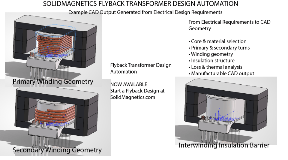
Early Engineering Access
SolidMagnetics is actively expanding and validating the flyback transformer design system with real engineering use cases.
Early users are encouraged to provide feedback on:
- Input workflow
- Calculation assumptions
- Candidate designs
- Generated outputs
- Missing requirements
- CAD geometry
- Desired documentation
- Unexpected results
- Additional features
Early Engineering Access currently provides:
30% off eligible SolidMagnetics designs with coupon code EARLYACCESS30 through November 12, 2026.
Engineering Review Is Still Required
Automated design does not remove the need for:
- Qualified engineering review
- Applicable safety analysis
- Semiconductor and control design
- PCB-layout verification
- Prototype construction
- Measured leakage and parasitics
- Temperature testing
- EMI testing
- Product certification
- Production validation
The generated design should be treated as an engineered design candidate that must be verified within the complete converter and end-product environment.
SolidMag Engineering Insight
Automation Expands Engineering Judgment
The most valuable function of magnetic-design automation is not replacing the engineer.
It is allowing the engineer’s design rules, limits, priorities, and judgment to be applied across far more possible transformer constructions than can reasonably be evaluated one at a time.
The final decision remains an engineering decision—but it can be supported by a much broader and more systematic design search.
28. Related Calculators, Guides, and Design Tools
Flyback transformer design involves several electrical, magnetic, thermal, winding, and parasitic calculations.
The following SolidMagnetics resources can be used to explore individual design relationships or continue into a complete automated transformer design.
Engineering Calculators
- Core Loss Estimator — estimate preliminary copper loss, core loss, and total magnetic-component loss from winding and core-loss inputs.
- Wire Size Calculator — estimate conductor area and preliminary wire size from RMS current and target current density.
- Saturation Checker — evaluate magnetic flux and saturation margin for a preliminary magnetic design.
- Engineering Calculators — browse the complete calculator directory.
These calculators provide first-pass engineering estimates. A complete flyback transformer still requires coordinated analysis of operating mode, magnetizing inductance, peak current, turns, gap, winding geometry, isolation, leakage, losses, temperature, mechanical construction, and semiconductor stress.
Related Engineering Guides
- Transformer Turns Ratio Explained
- Air Gap Design in Power Inductors
- How to Choose the Right Core Material
- Understanding Magnetic Saturation in Inductors
- What Is DCR in an Inductor? Understanding DC Resistance
- Inductor Temperature Rise Explained
- How Switching Frequency Affects Magnetics
- Ripple Current in Power Inductors: Design Guide, Equations, Examples & Calculator
- The Ultimate Guide to Inductor Design
Although several of these guides use inductors as their primary examples, the underlying magnetic principles—flux, gap, DCR, core loss, conductor loss, temperature, and frequency—also apply to flyback transformer design.
Design Automation
- Flyback Transformer Design Request — enter the electrical, thermal, mechanical, and design-priority requirements for an automated flyback transformer design.
- Magnetic Design Automation — choose between the currently available inductor and flyback transformer design systems and view future automation capabilities.
29. Conclusion
A flyback transformer is not simply a voltage-ratio device.
It is an energy-storage magnetic component that must coordinate:
- Magnetizing inductance
- Peak and RMS currents
- Primary and secondary turns
- Reflected voltage
- Core geometry and material
- Flux density
- Air gap
- Conductor selection
- Winding arrangement
- Isolation
- Leakage inductance
- Parasitic capacitance
- Core and copper loss
- Temperature rise
- Semiconductor stress
- EMI
- Mechanical construction
- Manufacturability
The design must remain valid across input voltage, output load, switching frequency, component tolerance, ambient temperature, startup, transient, and protection conditions.
No single equation or catalog table can establish a successful transformer by itself.
The electrical design, magnetic structure, winding construction, insulation system, parasitic behavior, thermal environment, and manufacturing process must agree.
A complete flyback transformer design follows an iterative process in which the electrical, magnetic, winding, thermal, mechanical, and manufacturing decisions are repeatedly verified and refined.
Modern automation can accelerate that process by evaluating more candidate combinations and operating conditions, but the resulting design must still be reviewed and verified within the complete converter and end product.
The strongest flyback transformer designs combine sound equations with practical construction, realistic tolerances, measured prototype behavior, and engineering judgment.
SolidMag Engineering Insight
A transformer design is complete only when its electrical performance, magnetic behavior, insulation, losses, temperature, parasitics, mechanical fit, and manufacturing process have all been verified together.
A mathematically correct transformer that cannot be safely manufactured, cooled, controlled, or validated is not a finished engineering design.
Ready to Evaluate a Flyback Transformer Design?
Enter your converter requirements and let SolidMagnetics evaluate the magnetic design, winding geometry, losses, thermal performance, and CAD construction.
Early Engineering Access: Save 30% with code EARLYACCESS30 through November 12, 2026.