Chapter 10 converts the magnetic platform selected in Chapter 9 into actual primary, secondary, and auxiliary conductors. The goal is not simply to choose a wire gauge. A practical conductor must carry the true RMS and harmonic current with acceptable DC and AC loss, fit the available winding window, satisfy insulation and termination requirements, and remain manufacturable.
← Previous Chapter
Next Chapter →
In This Chapter — Click to Expand
Table of Contents
1. Conductor Selection Starts with the Actual Current Waveform
Primary and secondary flyback currents are pulsed rather than steady DC. The primary typically conducts during the MOSFET ON interval, while the secondary conducts during the energy-delivery interval. Their peak values, RMS values, conduction times, harmonic content, and voltage stresses are therefore different.
Average current is useful for power balance, but winding heating is driven by RMS current and the effective winding resistance. At high switching frequency, that effective resistance can be substantially larger than the measured DC resistance because of skin effect, proximity effect, gap fringing, and current crowding.
SOLIDMAG ENGINEERING INSIGHT
Choose Conductors from Waveform, Frequency, and Construction
A conductor cannot be optimized from ampere rating or DCR alone. The correct choice depends on the actual current waveform, frequency spectrum, layer arrangement, field exposure, insulation system, window geometry, and thermal environment.
The best conductor is the one that minimizes total winding loss while remaining practical to wind, terminate, insulate, and manufacture.
2. Calculate Primary RMS Current
For an idealized DCM primary current that rises linearly from zero to peak current during duty cycle D:
For CCM, where the primary current rises from IMIN to IMAX during the ON interval:
The RMS current should be evaluated at every important operating corner because duty cycle, magnetizing inductance, switching frequency, and operating mode can all change the waveform.
3. Calculate Secondary Peak and RMS Current
Ignoring leakage and transition effects, the idealized secondary peak current immediately after primary switch turn-off is approximately:
For a DCM secondary current that decays approximately linearly from IS,PK to zero over secondary conduction fraction DS:
A low-voltage secondary may have only a few turns but can carry much higher peak and RMS current than the primary. Conductor area, terminations, rectifier connection geometry, and PCB current paths can therefore become dominant design constraints.
ENGINEERING CAUTION
Do Not Size the Secondary from Output DC Current
The 5 A DC output current of a flyback converter does not mean the transformer secondary carries a steady 5 A. The winding carries a pulsed current whose RMS value can be materially larger than the DC output current.
4. Auxiliary-Winding Current and Regulation Requirements
An auxiliary winding may provide controller bias, sensing, or an additional isolated output. Its conductor should be sized from the actual auxiliary load and conduction waveform rather than assumed negligible.
If the auxiliary winding is lightly loaded, copper loss may be small, but winding resistance and placement can still affect regulation. If it supplies significant continuous power, it should be treated as another output winding with its own RMS current, conductor area, rectifier stress, and thermal contribution.
The design should also define whether the auxiliary winding is primary-referenced or isolated, because this changes insulation and placement requirements.
5. First-Pass Copper Area from Current Density
A preliminary copper cross-sectional area can be estimated from an allowable current density:
| Variable | Meaning |
|---|---|
| ACU | Required copper cross-sectional area |
| IRMS | Winding RMS current |
| JALLOW | Selected allowable current density |
There is no universal current-density value for flyback transformers. The allowable value depends on winding location, cooling, insulation class, ambient temperature, maximum temperature rise, frequency, AC resistance, core geometry, and reliability target.
DESIGN ASSUMPTION
Current Density Is a Screening Tool
Use current density to establish a first-pass copper area. Final conductor acceptance must be based on calculated or measured winding loss and temperature rise in the finished transformer.
6. DC Winding Resistance and Temperature
A conductor of total copper length lCU has approximate DC resistance:
Conductor length includes more than active turns. Include winding turns, layer transitions, lead exits, pin or tab connections, and other current-carrying geometry.
Copper resistance rises with temperature:
Therefore room-temperature DCR should not be used as the final operating-loss value.
SOLIDMAG ENGINEERING INSIGHT
The Finished Conductor Length Matters More Than the Wire-Gauge Label
Two transformers using the same nominal wire gauge can have different DCR because of core geometry, mean turn length, layer count, leads, and termination geometry.
Conductor selection should therefore use the actual winding layout rather than only an AWG table.
7. Skin Effect and Skin Depth
At higher frequency, current tends to concentrate near the surface of a conductor. The skin depth of a good conductor can be approximated by:
As frequency increases, skin depth decreases. A conductor whose thickness or diameter is large compared with the relevant skin depth may not use its full copper area effectively for the AC components of the waveform.
The important frequency is not only the switching fundamental. Flyback current waveforms contain harmonics, and fast switching transitions can excite significantly higher-frequency current components.
As switching frequency increases, current no longer distributes uniformly through the conductor cross section. Skin depth establishes the approximate distance over which high-frequency current is concentrated near the conductor surface. Figure 10-1 compares this behavior in round wire and foil as conductor dimensions become large relative to the applicable skin depth.

When conductor diameter or foil thickness is small relative to skin depth, most of the available copper can participate in conduction. As the conductor becomes large relative to skin depth, current increasingly crowds near the surface and the effective AC resistance rises above the DC resistance. This is why simply increasing wire diameter or foil thickness does not necessarily reduce winding loss in a high-frequency flyback transformer.
Figure 10-1. Skin depth and current distribution in round wire and foil as conductor dimension becomes large relative to the applicable skin depth.
8. Proximity Effect in Multilayer Windings
Proximity effect is caused by magnetic fields from nearby conductors and winding layers. These fields force current toward particular regions of the conductor cross section, increasing effective AC resistance.
Proximity loss depends on:
- Number of winding layers
- Adjacent winding current
- Interleaving
- Conductor thickness
- Winding width
- Partial layers
- Harmonic content
- Gap fringing
- Primary-to-secondary placement
In many multilayer transformer windings, proximity effect can be more important than skin effect alone. A thick conductor that appears attractive from a DCR perspective can perform poorly when placed in a strong alternating field.
ENGINEERING CAUTION
Low DCR Does Not Guarantee Low AC Loss
Increasing conductor diameter or foil thickness can reduce DC resistance while increasing high-frequency current crowding. Optimize total winding loss, not only room-temperature DCR.
9. Conductor Options for Flyback Windings
| Conductor Type | Typical Advantages | Important Limitations |
|---|---|---|
| Single round wire | Simple, economical, easy to terminate | AC loss rises as diameter and frequency increase |
| Parallel round wires | More copper area with smaller individual diameter | Current sharing and physical placement must be controlled |
| Litz wire | Reduces skin and some proximity effects when correctly selected | Higher cost, larger insulated diameter, more complex termination |
| Foil | High copper area and low profile; useful for high-current windings | Can suffer strong proximity and gap-fringing loss |
| Triple-insulated wire | Can simplify some reinforced-isolation constructions | Larger outside diameter, higher cost, special termination requirements |
| Planar PCB / lead frame | Repeatable geometry, low profile, thermal integration | Capacitance, AC loss, current crowding, limited turn resolution |
The correct conductor type depends on current waveform, frequency, winding width, number of turns, isolation system, mechanical constraints, and manufacturing process.
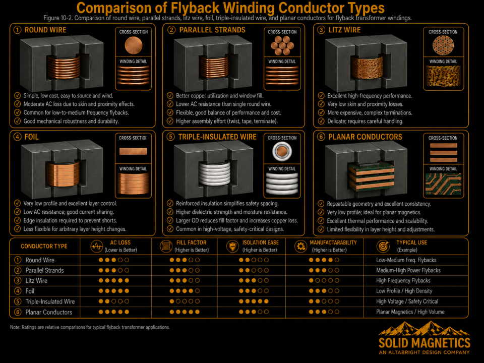
Figure 10-2. Comparison of round wire, parallel strands, litz wire, foil, triple-insulated wire, and planar conductors for flyback transformer windings.
10. Parallel Strands Are Not Automatically Litz Wire
Several ordinary insulated wires connected in parallel can reduce the diameter of each conductor and improve winding flexibility. However, parallel wires do not automatically provide the same current equalization as properly constructed litz wire.
If parallel strands occupy different magnetic-field positions, they can experience different induced voltages and unequal current sharing. The strands should be arranged so that their field exposure is as similar as practical and should be terminated symmetrically.
Litz wire deliberately transposes many insulated strands so that each strand occupies different positions within the bundle over its length. The strand diameter, number of strands, bundle construction, and operating frequency must all be selected appropriately.
11. Foil and High-Current Secondary Windings
Foil is attractive for low-voltage, high-current secondaries because it can provide substantial copper area in a controlled low-profile layer.
However, foil thickness, width, placement, and termination must be evaluated carefully. A foil that is too thick relative to skin depth or placed in a strong proximity or gap-fringing field can generate substantial AC loss.
The designer should evaluate:
- Foil thickness relative to skin depth
- Number of foil layers
- Field exposure from adjacent primary layers
- Distance from concentrated air gaps
- Insulation between foil layers
- Edge clearance and creepage
- Termination tabs and current spreading
- Rectifier and PCB connection geometry
SOLIDMAG ENGINEERING INSIGHT
High-Current Windings Are Often Limited by Geometry, Not Copper Area
Adding copper is easy in a spreadsheet. Fitting that copper into the actual bobbin while controlling AC loss, insulation, leakage, and termination temperature is the real design problem.
12. Window Fill Must Include Insulation and Manufacturing Space
The usable winding window established in Chapter 9 must contain the complete winding construction, not only bare copper.
Include:
- Conductor insulation
- Interwinding insulation
- Layer tape
- Margin tape or molded margins
- Triple-insulated wire outside diameter
- Sleeving
- Auxiliary windings
- Electrostatic shields
- Lead exits
- Manufacturing clearance
- Winding irregularity
A practical winding-fill check can be represented as:
The allowable fill factor depends on the winding process, conductor type, bobbin, insulation system, and production capability. Avoid designing to a theoretical 100% fill condition.
ENGINEERING CAUTION
Leave Manufacturing Margin
A winding that fits only in an ideal CAD cross section may fail in production because real wire placement, insulation overlap, bend radius, lead routing, and operator or machine tolerance consume additional space.
13. Terminations, Pins, Leads, and PCB Current Paths
The winding conductor is only one portion of the current path. Pins, leads, tabs, solder joints, PCB traces, and vias can add meaningful resistance and localized heating.
Verify:
- Pin current capability
- Number of parallel pins
- Lead length
- Solder-joint area
- Foil-tab geometry
- PCB copper width and thickness
- Via count and current sharing
- Mechanical strain relief
- Insulation stripping and termination method
A winding with acceptable copper loss can still fail thermally at a pin or PCB connection if the termination geometry is inadequate.
14. Worked Example — First-Pass Conductors for the Chapter 9 Design
DESIGN ASSUMPTION
Educational Conductor-Sizing Example
This example uses the current levels developed in the previous chapters and an illustrative current-density target. It is intended to establish first-pass copper area only. AC winding loss, exact layer geometry, and thermal verification still remain.
| Parameter | Primary | Secondary |
|---|---|---|
| RMS current | 1.18 A | 9.44 A |
| Illustrative current-density target | 4 A/mm² | 4 A/mm² |
| Approximate turns | 32 | 4 |
| Candidate mean turn length | 52 mm | 52 mm |
Step 1 — Estimate Primary Copper Area
Step 2 — Estimate Secondary Copper Area
The secondary requires approximately eight times the copper cross-sectional area of the primary under this simple current-density assumption.
Step 3 — Estimate Conductor Length
Step 4 — Estimate Room-Temperature DCR
Using an illustrative copper resistivity of 0.0175 Ω·mm²/m:
Step 5 — Estimate First-Pass DC Copper Loss
The equal result is a consequence of using the same current-density target and simplified geometry assumptions; it should not be interpreted as a universal transformer-loss balance.
Step 6 — Interpret the Result
| Quantity | Primary | Secondary |
|---|---|---|
| First-pass copper area | 0.295 mm² | 2.36 mm² |
| Estimated conductor length | 1.664 m | 0.208 m |
| Estimated room-temperature DCR | 98.7 mΩ | 1.54 mΩ |
| First-pass DC copper loss | 0.137 W | 0.137 W |
The primary may be realizable with one or more round conductors. The secondary likely requires parallel conductors, foil, or another high-current construction depending on the available winding width and AC-loss analysis.
The next winding-design iteration must check skin depth, proximity effect, number of layers, insulation, fringing fields, and actual winding temperature before any conductor is accepted.
SOLIDMAG ENGINEERING INSIGHT
First-Pass Copper Area Is Only the Starting Geometry
The current-density calculation produces a useful copper-area target, but the finished winding may require a completely different physical arrangement once AC loss, insulation, layer count, leakage, capacitance, and manufacturing are considered.
Chapter 11 will place these conductors into an actual winding arrangement and isolation structure.
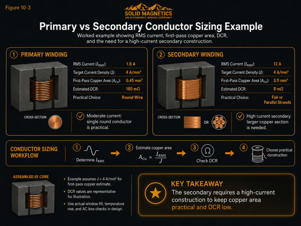
Figure 10-3. Worked primary and secondary conductor-sizing example showing RMS current, first-pass copper area, DCR, and the need for a high-current secondary construction.
15. Conductor Selection Checklist
- Primary, secondary, and auxiliary RMS currents are calculated from actual waveforms.
- Peak current and termination current are known.
- First-pass copper area is calculated from an explicit current-density assumption.
- Room-temperature DCR is estimated from actual conductor length.
- Temperature-corrected resistance will be evaluated.
- Skin depth and harmonic content are considered.
- Proximity effect and layer count are considered.
- Gap fringing is considered for conductors near the gap.
- Parallel strands are arranged for reasonable current sharing.
- Foil thickness and placement are checked where used.
- Triple-insulated wire outside diameter and termination requirements are included.
- Window fill includes insulation and manufacturing clearance.
- Pins, leads, solder joints, and PCB paths are checked.
- Final conductor choice will be verified by total winding loss and temperature.
16. Design Handoff to Winding Arrangement, Isolation, and Safety
At the end of Chapter 10, each winding should have a plausible conductor technology and copper-area target. The next task is to determine how those conductors are physically arranged on the bobbin while maintaining coupling, insulation, creepage, clearance, manageable capacitance, and manufacturability.
Chapter 11 will develop:
- Primary-secondary winding order
- Split-primary construction
- Interleaving
- Creepage and clearance
- Interwinding insulation
- Margin construction
- Triple-insulated wire
- Auxiliary placement
- Electrostatic shields
- Start and finish orientation
- Lead routing and pin assignments
SOLIDMAG ENGINEERING INSIGHT
Conductor Selection and Winding Arrangement Must Converge Together
A conductor choice can change the number of layers, winding width, insulation thickness, leakage, capacitance, and termination geometry. Chapter 11 may therefore force Chapter 10 conductor choices to be revised.
That iteration is normal and is part of creating a manufacturable transformer.
Technical References for This Chapter
Use conductor-manufacturer data, applicable wire standards, bobbin geometry, and winding-loss methods appropriate to the actual frequency and construction. Final AC resistance and temperature should be verified using the completed winding geometry and prototype measurements.
Related SolidMagnetics Resources
Ready to Design a Flyback Transformer?
Move from design theory to an automated magnetic design. Enter the converter requirements and evaluate a coordinated transformer candidate, winding geometry, loss estimates, thermal performance, and CAD output.
← Previous Chapter
Next Chapter →