Chapter 12 evaluates the parasitic elements created by the winding construction developed in Chapter 11. Leakage inductance stores energy that cannot transfer ideally to the secondary, while primary-to-secondary capacitance carries displacement current across the isolation barrier. Both parasitics shape MOSFET stress, clamp loss, ringing, regulation, common-mode EMI, and the practical winding arrangement.
← Previous Chapter
Next Chapter →
In This Chapter — Click to Expand
Table of Contents
1. Leakage Inductance and Capacitance Are Created by the Physical Winding
An ideal transformer assumes perfect magnetic coupling and no capacitance between windings. A real flyback transformer has neither property. Some magnetic field links only one winding, creating leakage inductance, and the primary and secondary conductors form an unintended capacitor across the isolation barrier.
These parasitic elements are strongly controlled by winding geometry. Greater primary-secondary separation usually reduces capacitance but increases leakage. Closer coupling and interleaving usually reduce leakage but increase capacitance. The winding design must therefore balance both rather than minimizing one parasitic independently.
SOLIDMAG ENGINEERING INSIGHT
Leakage and Capacitance Are Opposing Geometry Tradeoffs
The construction that produces the lowest leakage inductance is rarely the construction that produces the lowest primary-to-secondary capacitance.
The best flyback winding balances semiconductor stress, clamp loss, common-mode EMI, isolation, copper loss, regulation, and manufacturability.
2. Coupling Coefficient and the Leakage-Inductance Model
For a simplified linear two-winding transformer, the magnetic coupling coefficient is:
| Variable | Meaning |
|---|---|
| k | Magnetic coupling coefficient |
| M | Mutual inductance |
| LP | Primary self-inductance |
| LS | Secondary self-inductance |
A perfectly coupled ideal transformer would have k = 1. A practical transformer has a coupling coefficient below unity.
In a simplified two-winding model, primary-referred leakage inductance can be written as:
or:
Real multiwinding transformers can require a more complete equivalent circuit, but these equations provide a useful first-order view of how imperfect coupling appears electrically.
3. Leakage Energy at MOSFET Turn-Off
At the instant the MOSFET turns OFF, the magnetizing energy is intended to commutate to the secondary winding. Leakage energy is different because it is associated with flux that does not link the secondary effectively.
If that leakage energy is dissipated once per switching cycle in a passive clamp or snubber, a first-order loss estimate is:
This represents a simplified dissipative case. Active-clamp and energy-recovery circuits can return some of the leakage energy instead of dissipating all of it.
ENGINEERING CAUTION
Leakage Energy Can Become a Significant Efficiency Penalty
Leakage energy increases with the square of peak current. A modest increase in peak current can therefore produce a disproportionately large increase in clamp loss and switch stress.
4. Drain-Voltage Overshoot, Clamp Action, and Ringing
Inductance generates voltage when current changes rapidly:
The ideal flyback MOSFET drain plateau is approximately the input voltage plus the reflected output voltage. Leakage inductance adds a transient overshoot above that plateau.
The measured drain waveform can additionally contain:
- Leakage-inductance spike
- Clamp or snubber voltage
- Ringing between leakage inductance and parasitic capacitance
- PCB loop inductance
- MOSFET output capacitance
- Transformer winding capacitance
- Diode and layout parasitics
A useful first-order ringing-frequency estimate is:
where CEQ is the effective capacitance participating in the ringing mode. The actual resonant network should be identified from the measured circuit rather than assumed from one component value.

Figure 12-1. Flyback MOSFET turn-off waveform showing ideal reflected-voltage plateau, leakage-inductance overshoot, clamp action, and high-frequency ringing.
5. How Winding Geometry Controls Leakage Inductance
Leakage inductance is primarily a winding-geometry problem. It increases as more magnetic field exists in regions that are not shared by the coupled windings.
Leakage tends to increase with:
- Greater primary-secondary spacing
- Thicker insulation barriers
- More winding layers
- Narrow or partial winding layers
- Different primary and secondary winding widths
- Long winding leads
- Separated auxiliary or secondary windings
- Poor alignment of coupled sections
Leakage can often be reduced by:
- Using the available winding width effectively
- Reducing unnecessary winding layers
- Minimizing unnecessary spacing between coupled windings
- Aligning primary and secondary winding widths
- Using split-primary construction where appropriate
- Interleaving winding sections
- Reducing lead length and loop area
- Placing the highest-power secondary close to the primary
SOLIDMAG ENGINEERING INSIGHT
Leakage Reduction Begins with the Winding Stack
A clamp circuit can manage the consequences of leakage inductance, but it does not eliminate the leakage itself. The first opportunity to reduce leakage is in the physical transformer construction.
6. Interleaving Reduces Leakage but Usually Increases Capacitance
Interleaving divides primary and secondary windings into multiple sections so that their magnetomotive-force distributions overlap more closely. This can substantially reduce leakage inductance.
However, interleaving also increases the physical interface area between primary and secondary conductors. That interface area contributes to primary-to-secondary capacitance.
A useful first-order capacitance trend is represented by the parallel-plate relationship:
where A is effective overlap area, d is dielectric separation, and ε is the dielectric permittivity. Actual transformer capacitance is distributed and geometry dependent, but this relationship illustrates the trend: more overlap and smaller separation generally increase capacitance.
| Winding Strategy | Leakage Tendency | Capacitance Tendency | Manufacturing Complexity |
|---|---|---|---|
| Simple primary-secondary | Higher | Lower | Lowest |
| Split primary | Lower | Higher | Moderate |
| More aggressive interleaving | Lowest tendency | Highest tendency | Highest |
ENGINEERING CAUTION
Do Not Optimize Leakage Without Measuring Common-Mode EMI
Interleaving may improve drain overshoot and clamp loss while making conducted or radiated common-mode emissions worse. Evaluate the complete converter before accepting the winding.
7. Primary-to-Secondary Capacitance and Displacement Current
The primary and secondary windings form an unintended capacitance across the isolation barrier. Rapid voltage transitions drive displacement current through this capacitance:
where CPS is the effective primary-to-secondary capacitance and VPS is the voltage difference across it.
The charge transferred by a voltage step is approximately:
Even a capacitance of only a few tens of picofarads can produce large short-duration currents when dv/dt is high.
SOLIDMAG ENGINEERING INSIGHT
Small Capacitance Can Carry Large Switching Current
The average capacitance value may look insignificant, but common-mode current is driven by capacitance multiplied by dv/dt. Fast switching can therefore make transformer capacitance one of the dominant EMI paths.
8. Common-Mode EMI Through the Transformer
In an isolated flyback converter, common-mode noise can cross the transformer through parasitic capacitance even though there is no intentional conductive connection between primary and secondary.
A simplified common-mode current relationship is:
The resulting current can return through:
- Secondary-to-earth or chassis capacitance
- Output cables
- Load capacitance
- Safety Y capacitors
- Heatsink capacitance
- Measurement equipment
- Parasitic capacitance back to the primary or earth
The actual path must be identified for the complete product. Transformer capacitance is only one element in the common-mode loop.
FIGURE 12-2 PLACEHOLDER

Figure 12-2. Simplified flyback common-mode noise path showing switch-node dv/dt, primary-to-secondary capacitance, secondary displacement current, and return path through parasitic or safety capacitance.
9. Winding Voltage Distribution and Layer Pairing
Capacitance alone does not determine common-mode current. The voltage difference and voltage distribution between adjacent winding layers also matter.
Two primary-secondary interfaces with the same physical capacitance can produce different common-mode currents if one pair experiences a larger instantaneous voltage difference.
Advanced winding optimization can therefore consider:
- Which primary layer is adjacent to the secondary
- Start and finish orientation
- Voltage distribution along each winding
- Auxiliary winding location
- Split-primary connection order
- Shield placement and reference
The objective is to reduce the effective voltage difference across high-capacitance interfaces without compromising safety or producing a closed conductive turn.
ENGINEERING CAUTION
Layer Voltage Distribution Is Construction Specific
Do not assume that every interleaved winding improves EMI. The actual voltage distribution across adjacent layers must be considered together with capacitance and winding polarity.
10. Electrostatic Shields and Y-Capacitor Paths
An electrostatic shield can redirect some displacement current away from the secondary. A safety-rated Y capacitor can intentionally provide a controlled common-mode return path in some end products.
These techniques require careful safety and EMI design.
- A transformer shield must not form a closed conductive turn around the core.
- Shield connection point and winding location affect the current path.
- Any capacitor crossing the isolation barrier must meet the applicable safety requirements.
- Added capacitance can increase touch current or leakage current.
- The complete product—not only the transformer—must be evaluated for compliance.
ENGINEERING CAUTION
Isolation Components Are Safety-Critical
Do not add a Y capacitor or shield connection simply to improve an EMI scan. Use appropriately rated components and verify the resulting leakage current, isolation, fault behavior, and applicable product-safety requirements.
11. Differential-Mode and Common-Mode EMI Are Different Problems
Leakage ringing and common-mode capacitive current can both create high-frequency emissions, but they travel through different paths.
| Noise Type | Typical Source | Typical Current Path | Transformer Influence |
|---|---|---|---|
| Differential mode | Switching ripple, leakage ringing, diode commutation | Out and back through the power conductors | Leakage inductance, winding resistance, ringing |
| Common mode | High dv/dt nodes and parasitic capacitance | Both power conductors relative to chassis/earth or another reference | Primary-secondary capacitance, shields, winding voltage distribution |
A change that improves one mode can worsen the other. For example, stronger interleaving may reduce leakage-related differential ringing while increasing common-mode current through higher interwinding capacitance.
12. Measuring Leakage Inductance, Capacitance, and Ringing
Parasitics should be measured under defined conditions so that design iterations can be compared meaningfully.
Primary-Referred Leakage Inductance
A common method is to short the secondary and auxiliary windings appropriately and measure inductance from the primary:
Record the test frequency, signal level, fixture, shorting method, and winding connections. Fixture inductance can become significant when leakage is small.
Primary-to-Secondary Capacitance
Capacitance is commonly measured by tying together the terminals on each side of the isolation barrier and measuring between the primary-side group and secondary-side group. The exact method should be documented because shields, core clips, auxiliary windings, and fixture capacitance can alter the result.
### Converter Waveforms
Measure MOSFET drain overshoot, ringing frequency, clamp voltage, secondary ringing, and common-mode current under representative line and load conditions.
A current probe around both output conductors together can help identify common-mode current because differential load current cancels ideally in the probe while common-mode current adds.
SOLIDMAG ENGINEERING INSIGHT
Measure the Parasitics in the Same Construction You Plan to Manufacture
Leakage and capacitance are physical-geometry results. A hand-wound prototype with different layer placement, insulation thickness, or lead routing can produce misleading measurements.
Parasitic targets should be verified on representative production-intent transformers.
13. Worked Example — Leakage Energy, Ringing, and Common-Mode Current
DESIGN ASSUMPTION
Educational Parasitic Example
The values below are illustrative and are intended to show the scale of the effects. Actual clamp loss, ringing capacitance, common-mode current, and EMI depend on the complete converter and measurement setup.
| Parameter | Illustrative Value |
|---|---|
| Primary-referred leakage inductance | 1.5 µH |
| Peak primary current | 3.06 A |
| Switching frequency | 100 kHz |
| Effective ringing capacitance | 150 pF |
| Primary-secondary capacitance | 40 pF |
| Illustrative voltage slew rate | 10 V/ns |
| Illustrative primary-secondary voltage step | 500 V |
Step 1 — Calculate Leakage Energy
Step 2 — Estimate Dissipative Clamp Loss
If all leakage energy were dissipated every cycle, the transformer parasitic alone would create roughly 0.70 W of clamp-related loss.
Step 3 — Estimate Ringing Frequency
Step 4 — Estimate Instantaneous Capacitive Current
This is a short-duration displacement-current estimate, not a 0.40 A DC current. It illustrates why only tens of picofarads can matter at fast switching edges.
Step 5 — Calculate Charge Moved Across the Isolation Capacitance
Each large switching transition can therefore move tens of nanocoulombs through the parasitic isolation capacitance under the stated assumptions.
| Calculated Quantity | Result |
|---|---|
| Leakage energy per cycle | 7.02 µJ |
| Simplified dissipative leakage loss | 0.702 W |
| Estimated ringing frequency | 10.6 MHz |
| Peak illustrative displacement current | 0.40 A |
| Charge moved for 500 V step | 20 nC |
SOLIDMAG ENGINEERING INSIGHT
A Few Microhenries and Picofarads Can Dominate High-Frequency Behavior
Parasitic values that appear small beside the main 147 µH magnetizing inductance or the converter power can still dominate switching spikes, clamp loss, and common-mode EMI.
This is why transformer parasitics must be designed deliberately rather than treated as measurement surprises.
Transformer parasitics can be translated directly into measurable converter behavior. Leakage inductance stores energy that must be absorbed or recovered at turn-off, while primary-to-secondary capacitance couples high-dv/dt switching energy across the isolation barrier.
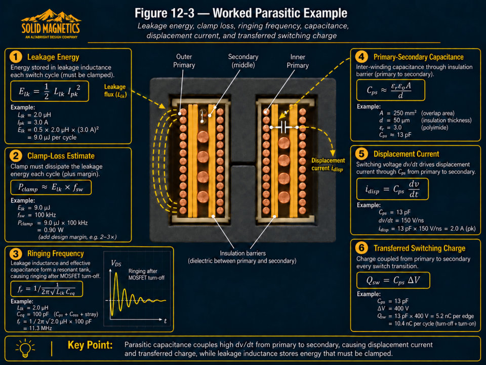
This worked example shows how leakage inductance and parasitic capacitance influence clamp dissipation, ringing frequency, displacement current, and transferred switching charge. These effects are determined by the physical winding geometry and should be evaluated together with isolation, winding arrangement, semiconductor stress, and EMI performance.
Figure 12-3. Worked parasitic example showing leakage energy, clamp-loss estimate, ringing frequency, primary-secondary capacitance, displacement current, and transferred switching charge.
14. Optimize Leakage, Capacitance, and EMI Together
| Design Change | Leakage Effect | Capacitance Effect | Possible EMI / Loss Consequence |
|---|---|---|---|
| Move primary and secondary closer | Lower | Higher | Lower leakage spike but potentially higher common-mode current |
| Increase insulation spacing | Higher | Lower | Lower capacitance but greater clamp stress |
| Split primary | Lower | Higher | Often useful compromise; verify CM EMI |
| More interleaving | Lower | Higher | Can reduce leakage loss while increasing CM coupling |
| Use electrostatic shield | Geometry dependent | Redirects effective coupling | Can improve CM path if connected correctly |
| Shorten leads | Lower local stray L | Little direct C change | Reduces ringing and radiated loop area |
The optimization target should be expressed in measurable converter quantities such as maximum drain overshoot, clamp loss, primary-secondary capacitance, conducted EMI, common-mode current, regulation, efficiency, and temperature.
SOLIDMAG ENGINEERING INSIGHT
Do Not Specify Only ‘Minimum Leakage’
A useful transformer specification defines an acceptable leakage range together with capacitance, insulation, winding construction, and converter-level performance requirements.
Minimum leakage without a capacitance limit can push the transformer toward an EMI-unfriendly construction.
15. Leakage, Capacitance, and EMI Design Checklist
- Primary-referred leakage inductance is estimated and measured.
- Leakage energy is calculated at worst-case peak primary current.
- Clamp or snubber loss is evaluated.
- MOSFET drain overshoot remains below the design limit with margin.
- Ringing frequency and damping are measured.
- Primary-secondary capacitance is measured using a documented method.
- Common-mode current paths are identified.
- Interleaving is evaluated against both leakage and capacitance.
- Winding voltage distribution is considered.
- Electrostatic shields cannot form a closed turn.
- Any isolation-barrier capacitor is safety rated and product compliant.
- Differential-mode and common-mode EMI are evaluated separately.
- Parasitic measurements use representative production-intent transformers.
- The final winding stack is updated if converter measurements fail.
16. Design Handoff to Copper Loss, Core Loss, and Thermal Design
At the end of Chapter 12, the winding construction has been evaluated not only for safety and manufacturability but also for the parasitic elements it creates. The next step is to calculate the total losses and resulting temperature rise.
Chapter 13 will combine:
- Temperature-corrected winding DCR
- Skin and proximity effects
- Gap-fringing winding loss
- Core material loss
- Flux waveform
- Core volume
- Leakage/clamp-related thermal effects where appropriate
- Lead and termination loss
- Thermal resistance and cooling conditions
SOLIDMAG ENGINEERING INSIGHT
Parasitics Become Part of the Thermal Design
Leakage inductance and capacitance are usually discussed as switching and EMI problems, but both can also increase loss in the clamp, MOSFET, windings, and surrounding circuitry.
Chapter 13 converts the electromagnetic design into a complete loss and temperature budget.
Technical References for This Chapter
Texas Instruments — Flyback transformer design considerations for efficiency and EMI
Texas Instruments — An Engineer’s Guide to Low EMI in DC/DC Regulators
Power Integrations — LinkSwitch-3 Family Design Guide, AN-61
Use the actual converter schematic, clamp topology, transformer construction, EMI test setup, and applicable safety requirements when translating these concepts into a production design.
Related SolidMagnetics Resources
Ready to Design a Flyback Transformer?
Move from design theory to an automated magnetic design. Enter the converter requirements and evaluate a coordinated transformer candidate, winding geometry, loss estimates, thermal performance, and CAD output.
← Previous Chapter
Next Chapter →